
Ho Wei Hao
Year 4 Electrical Engineering
A0240152X
2. Radiation Monitoring System
2.1 Job Scope
The objective of my work is to ensure that the payload can detect and record radiation levels accurately, and that the components used to fulfil the objective are suitable for space applications. My scope of work consists of the following tasks:
1. Radiation Sensor Operations
As part of mission objectives, the payload will be monitoring and storing radiation counts. A radiation sensor has to be powered and its output read and stored.
2. High Voltage PCB Design
Custom Printed Circuit Boards (PCB) were designed to provide the high power requirements of the radiation sensor and to process its output. Sufficient clearance is required between the high voltage lines from the rest of the signal conditioning circuit. This prevents inference between the two systems that can break down the entire payload.
## 2.2 Design Requirements
The payload requires certain specifications to be met to operate as intended. Since the interim report, the list has gained new specifications to meet.
| Feature | Specification | Reasoning |
|---|---|---|
| Operating Voltage | 5V | Assumption of 5V provided by flight provider. |
| Current Consumption | <2A | Assumption of 2A maximum provided by flight provider. Current is shared with low voltage board developed by Sowmya. |
| Radiation Sensor | Detects alpha, beta and gamma particles | Monitor the particles responsible for SEE. |
| Signal processing | Microcontroller gets triggered once per signal for accurate detection | Ensure radiation is correctly recorded by the microcontroller. |
| Microcontroller | Radiation-Hardened | Provide reliable data storage throughout the mission. |
| High and low voltage clearance | Ensure voltage lines do not interfere with each other | Avoid eletrical damage and compromising other systems on the same payload or satellite. |
| Signal interference | Signals only travel through the signal net | Prevent unwanted noise in other nets and prevent unwanted distortions to signal. |
| Space suitability | Total Mass Loss (TML) and Collected Volatile Condensable Materials (CVCM) of each component do not exceed 1% and 0.1% respectively (Kern, 2019) | High CVCM values indicate that unwanted vapours will condense on the payload and its adjacent components, which may contaminate or interfere with operations of nearby sensitive equipment that need cleanliness (Kern, 2019). TML must also be low as the vaporised material may condense on surrounding equipment and hamper their operations (Kern, 2019). |
| Thermal resistance | Components must be able to operate reliably from -25°C to 70°C (FalconUsersGuide, 2021). | PCB must pass the thermal cycling test for qualifications testing. More details on thermal cycling test will becovered by Mingchuan. |
| Mechanical robustness | PCB must be able to operate reliably after intense vibrations from all 3 axes experienced during launch. | PCB must pass the random and sine vibrations test for qualifications testing. More details on vibration tests will be covered by Mingchuan. |
Table 2-1 Design Specifications Table
2.3 Design Specifications
Only the ZSOM-M01 microcontroller and the GM tube persisted into the final design.
2.3.1 Unchanged Components
2.3.1.1 Microcontroller
Design Choice
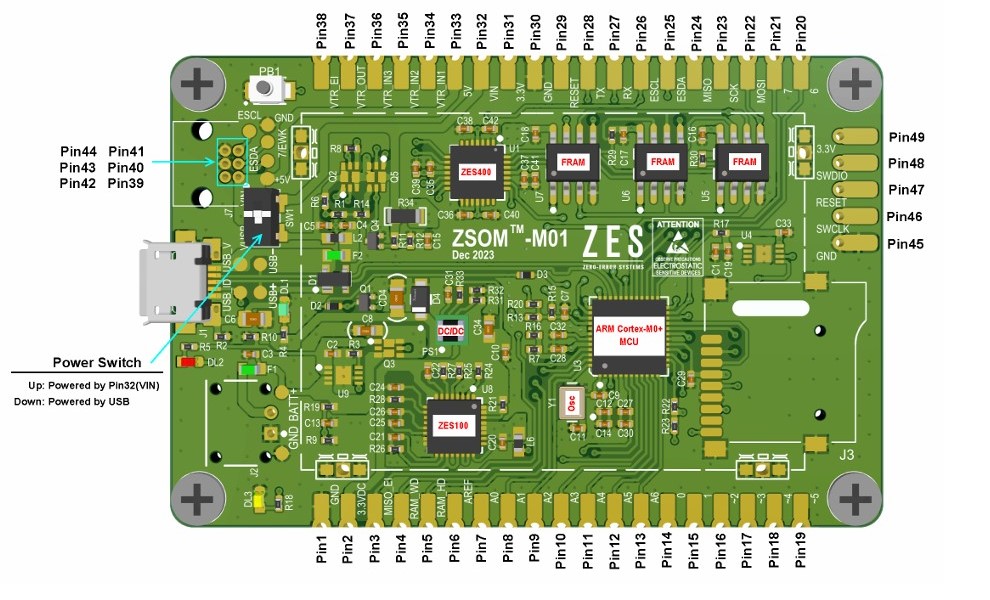
Fig 2-2 ZSOM-M01 board (Zero Error Systems, 2024b)
The ZSOM-M01 remained on the final design due to its reliability in storing data of the mission. This trait is supported by its radiation hardened status, Triple Modular Redundancy configuration and the Error Detection and Correction functionality (Zero Error Systems, 2024b). Since our main mission consists of a memory corruption experiment of Atmega32U4 microcontrollers, the ZSOM-M01 provides the robust foundation for collecting data for further analysis.
The detailed explanation for choosing ZSOM-M01 can be found in appendix B1.
The ZSOM-M01 can operature within the temperature range of -40°C to 105°C, allowing it to operate normally within the temperature range for the thermal cycling test (Zero Error Systems, 2024b).
Design Implementation
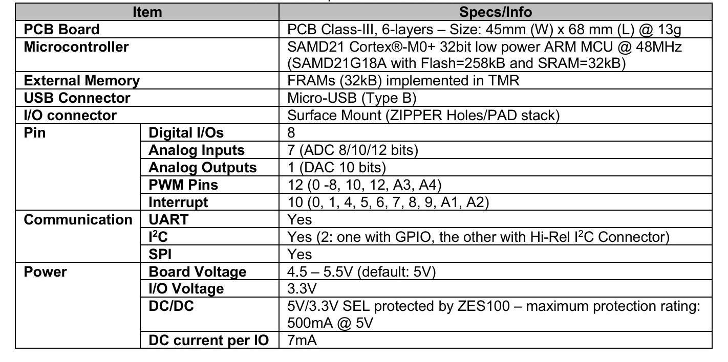
Fig 2-3 Pinout of ZSOM-M01 (Zero Error Systems, 2024b)
The ZSOM-M01 pins that were planned to be used in the circuit were altered during prototyping. The Geiger-Müller (GM) tube now sends the detected signal at unpredictable intervals to the ZSOM-M01 via D4 interrupt pin. This allows the ZSOM-M01 to count the signal immediately in the midst of its other operations, ensuring that the signals are recorded accurately.
The PWM pin from the ZSOM-M01 is no longer needed to control the converter. This further simplifies the circuit. The new connection will be shown in the later circuit design.
2.3.1.2 GM Tube
Design Choice
The GM tube remained on the final design as it could provide robust signals as an indication of the radiation levels it experienced. Detailed explanation of its choice over other detectors can be found in the appendix B2.
Design Implementation
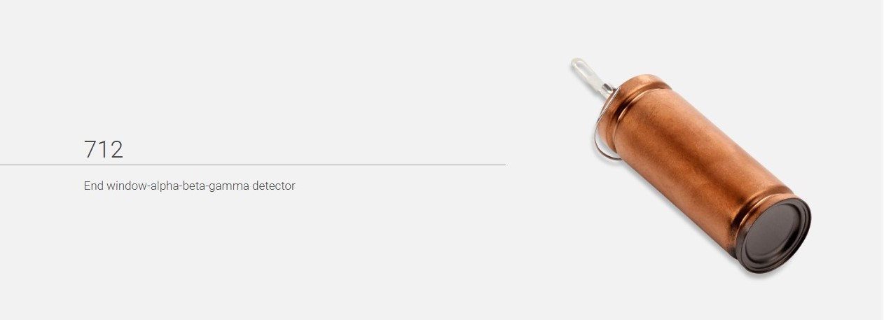
Fig 2-4 LND712 GM Tube (LND. Inc., n.d.)
The LND 712 is chosen for our purposes. It requires between 450V to 650V to operate, which can be supplied easily with a DC-to-DC converter, making it easy to integrate. The connections required are also very simple, requiring two resistors and a 50pF capacitor. The GM tube can also operate between -40°C to 70°C, hence it can operate normally during the thermal cycling test (LND. Inc., n.d.).
2.3.2 New Components
Several new components are added to the final design.
2.3.2.1 DC-DC Converter
Design Choice
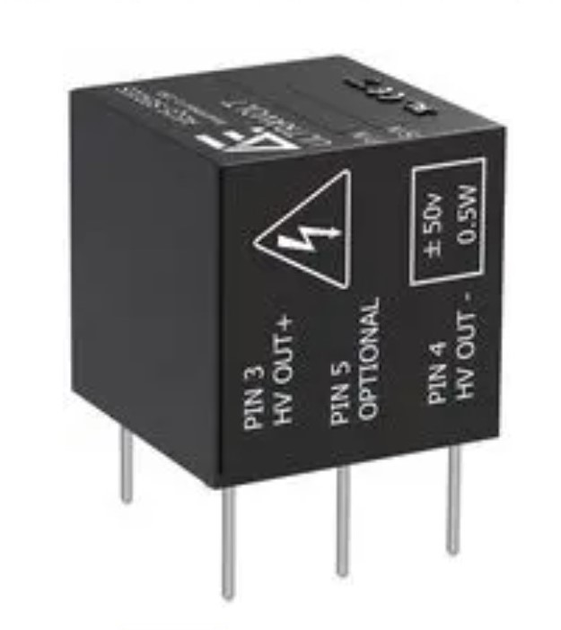
Fig 2-5 AEQ5-600FL0.5 Converter (Element14, 2025)
The AEQ5-600FL0.5 provides a reliable input of around 600V to the GM tube, allowing the Gm tube to operate optimally without being vulnerable to small changes in load that may disrupt its poeer supply. This prevents over-voltage damage to the GM tube, and allows it to work at its optimal operating voltage. It can also operate between -25°C to 70°C, hence it can operate normally during the thermal cycling test (Element14, 2025).
Fig 2-6 Advanced Energy’s Senior Engineer confirming casing material (E. Wang, personal communication, Mar 03, 2025)
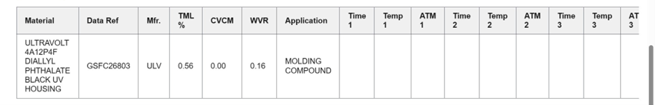
Fig 2-7 TML and CVCM values from NASA’s Outgassing Database (National Aeronautics and Space Administration, n.d.)
According to the senior engineer from the Advanced Energy, the converter’s casing is made of black diallyl phthalate (E. Wang, personal communication, Mar 03, 2025).The material has TML and CVCM values of 0.56% and 0.00%, making it suitable for use in space applications (National Aeronautics and Space Administration, n.d.).
Design Implementation
The converter is powered by 5V and accepts a control signal ranging from 0V to 5 V to provide a maximum output of up to 600V. In the circuit design, the control pin is tied to 5V in the PCB. This simplifies the circuit design and reduces the workload of the ZSOM-M01 to control the converter.
2.3.2.2 Thermal Pad
Design Choice
As the converter experiences a significant rise in temperature during operation, effective heat management is required to ensure its continued optimal operation in space. This is because there is no air in the vacuum of space to remove heat from the converter via convection. Thermally conductive but electrically insulating thermal pad is used to conduct heat from the converter to the aluminium shielding of the payload, while maintaining electrical isolation to prevent short circuits. This utilises the high volume of the shielding as an effective heatsink to radiate heat away in space, thereby preventing the converter from overheating and getting damaged.
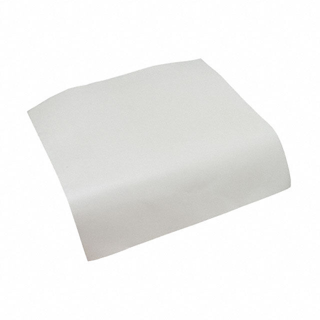
Fig 2-8 Figure 7.SIL-PAD 2000 Thermal Pad (DigiKey, 2025)
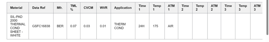
Fig 2-9 Sil-Pad Outgassing Data (National Aeronautics and Space Administration, n.d.-b)
The SIL-PAD 2000 thermal pad was chosen as it has 0.07% and 0.03% as its TML and CVCM value respectively (National Aeronautics and Space Administration, n.d.-b). This makes it acceptable for space applications.
Its high thermal conductivity of 3.5W/m-K helps it efficiently conduct heat away from the converter. It also has adhesive on one side, making it easier to secure in the payload. Furthermore, it can withstand temperatures from -60°C to 200°C, hence it will not receive damage from the thermal cycling test (DigiKey, 2025).
Design Implementation
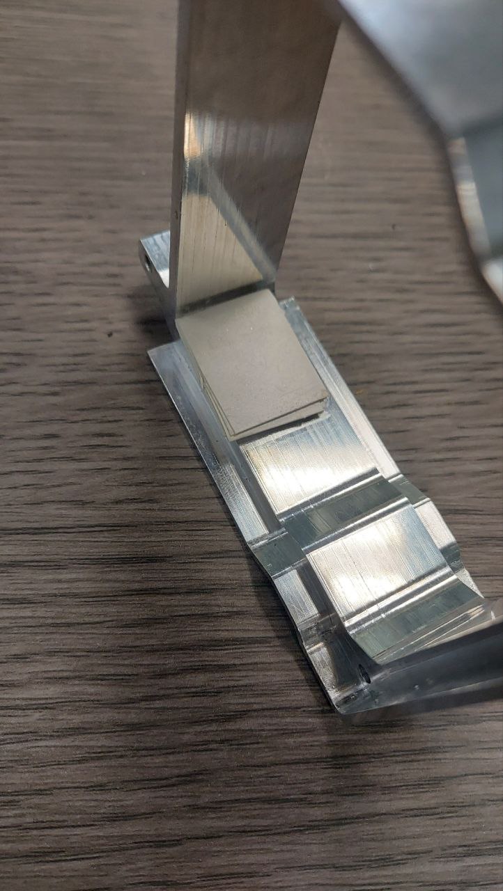
Fig 2-10 Thermal pad applied to the inside of the shielding
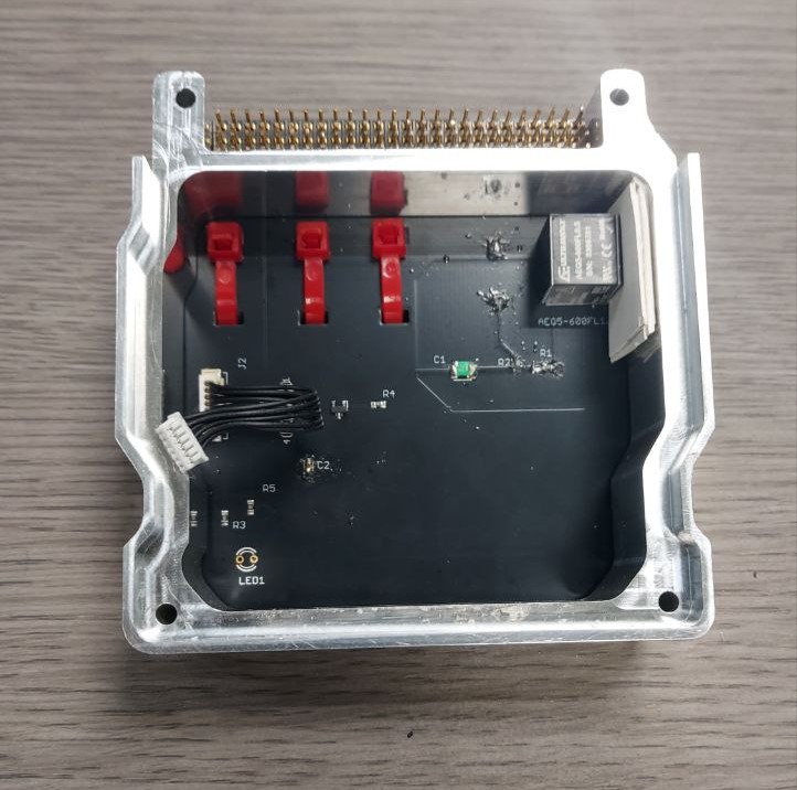
Fig 2-11 Converter pressed firmly on the thermal pad
Six 20mm by 25mm pieces of thermal pad were stacked to the left side of the shielding, so that the converter presses firmly onto the thermal pad when the PCB is mounted onto the shielding. This maximises the area of contact and minimises any gaps between the converter and the material, transferring heat effectively to the shielding in the vacuum of space.
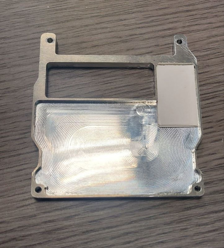
Fig 2-12 Thermal pad applied to underside of shield cover
Three pieces of 22mm by 36mm of thermal pad were adhered on the top cover of the shielding, where the pins of the converter are situated. While the pins of the converter have sufficient clearance from the shielding, this further ensures that the pins, especially the 500V output pin of the converter, will be electrically isolated from the shielding.
2.3.2.3 Cable Tie
Design Choice
Cable ties were needed to physically fasten the GM tube to the PCB. This is to prevent the GM tube from receiving damage when experiencing violent vibrations during launch.

Fig 2-13 Pan-ty Cable Tie Halar Maroon (Mouser Electronics, 2025)
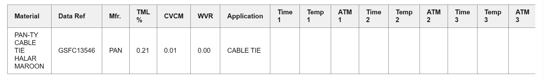
Fig 2-14 Cable Tie Outgassing Data (National Aeronautics and Space Administration, n.d.-c)
The Pan-ty Cable Tie Halar Maroon was selected for its low outgassing properties, as compared to other cable-ties. Its TML and CVCM values were 0.21% and 0.01%, within the acceptable range for space applications (National Aeronautics and Space Administration, n.d.-c).
It can also withstand the temperature range of -60°C to 125°C, thus avoiding any damage during the thermal cycling test (Panduit, n.d.).
Design Implementation
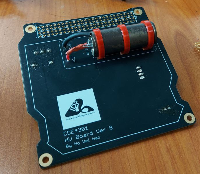
Fig 2-15 Cable tie securing GM tube to PCB
The ties will be looped through holes designed on the PCB and tightened around the GM tube and PCB, firmly securing the GM tube in place and ensuring its mechanical stability throughout the launch and the mission.
2.4 Design Process
2.4.1 Proof of Concept
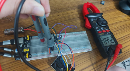
Fig 2-16 Breadboard prototype circuit
The components were first tested in a proof of concept to refine component selection. Once the proof-of-concept worked, the process of PCB design started.
Details on the proof-of-concept and its testing can be found in appendix B3.
2.4.2 Custom PCB Design
2.4.2.1 PCB Schematic
Based on the proof of concept, PCB schematic was designed as follows: Link
The overall design of the high voltage circuit remains unchanged since the proof-of-concept stage, except for the specific values of the resistors and capacitors.
Detailed explanations for the circuit design can be found in the appendix B4.
2.4.2.2 PCB Layout
Several iterations of the PCB were designed for testing hypotheses and aligning design goals with the other teammates.
Detailed breakdown of each iteration can be found in appendix B5.
2.4.2.2.1 Layout considerations
Considerations while designing the PCB are listed below.
High-voltage and Low-voltage clearance
Internal conductors in the PCB like traces and external uncoated components on the PCB such as vias and exposed pads need to be 0.0025mm and 0.00305mm apart per voltage of potential difference respectively. This is to prevent signal interference or electrical leakages (JHDPCB, 2024).
For a maximum of 600V of potential difference,
Internal conductors clearance = 0.0025mm/v * 600V = 1.5mm
External uncoated components = 0.00305mm/v * 600V = 1.83mm
Hence, internal conductors and external components need to be at least 1.5mm and 1.83mm apart respectively.
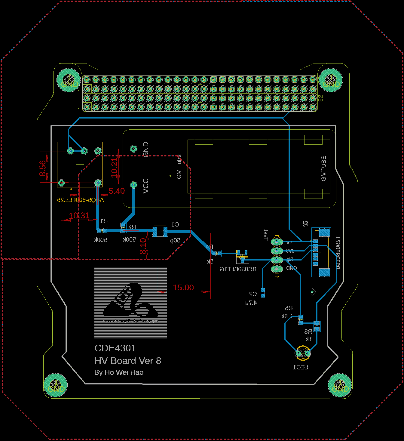
Fig 2-17 High voltage lines sufficient distances away from any low voltage line and components (Clearances marked in red)
Ground Pour
Clearance was based on the above calculations also ensured between the ground plane and the high voltage lines to avoid electrical short-circuits or arcing due to the high potential difference.
GM Tube Placement
Since the GM tube receives radiation particles from its mica window, its window is oriented to face the right of the PCB which is unblocked by any component. This allows the GM tube to operate unhindered.
Electrical Alignment
The location of the pinstack was aligned with the low-voltage PCB developed by Sowmya. The high-voltage PCB needs to receive 5V and 3.3V power from the low voltage PCB, while sending GM tube signals to the ZSOM-M01 on the low-voltage PCB. To achieve this, a 6-header picoblade wire is used to connect the two boards. A 6-header molex male connector was placed on the right underside of the board to be closer to the other one on the low-voltage board. This allows a shorter picoblade wire to be used.
Mechanical Alignment
The PCB has to be mechanically mounted into the payload. Hence, the shape of the PCB and pinstack location was coordinated with Mingchuan who developed the shielding and the mounting. The placement of the GM tube was also coordinated to ensure that the entire payload will be shielded except for the GM tube for it to receive radiation particles.
2.4.2.2.2 Final Layout The final PCB design incorporating the design considerations is shown below:
Fig 2-18 Final Layout
2.4.5 Signal Detection Code
A simple arduino code was also developed to allow the ZSOM-M01 detect signals from the GM tube. The ZSOM-M01 will count the signals for a minute to provide the radiation reading as counts per minute. The full code can be found in appendix B6.
The code was then passed to Richard to integrate into the ZSOM-M01 firmware.
2.4.6 Signal Conditioning Tuning
To ensure that inherent capacitances in the PCB was accounted for in the final prototype, the lowpass filter on the signal net on the latest PCB iteration was tuned.
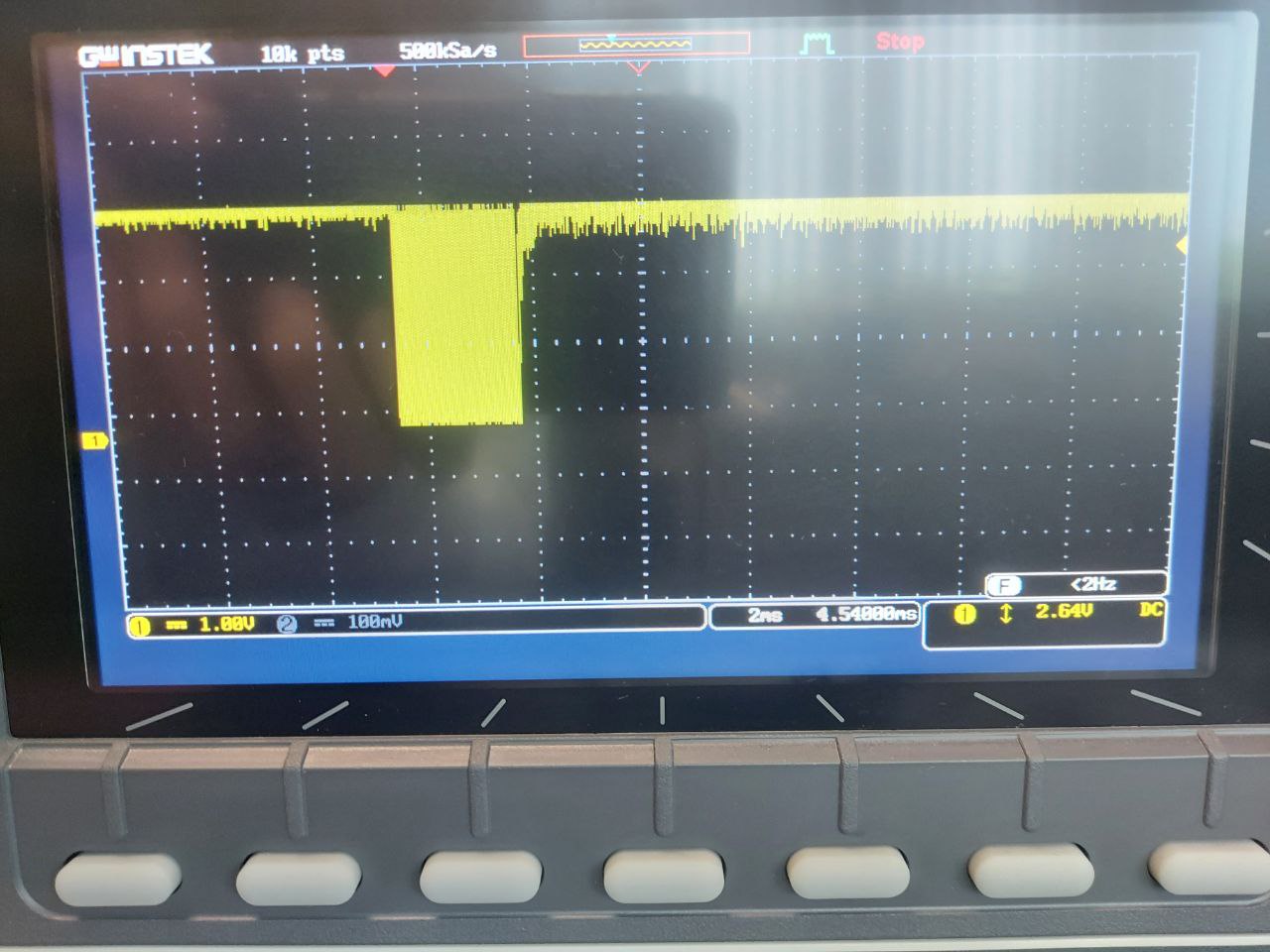
Fig 2-19 Unfiltered Signal
The raw incoming signal from the GM tube is very noisy, causing hundreds of false counts for each signal. This added up to thousands counts per minute, which was several times more than the normal background radiation of around 5 to 60 counts per minute (ECOTEST, 2025).
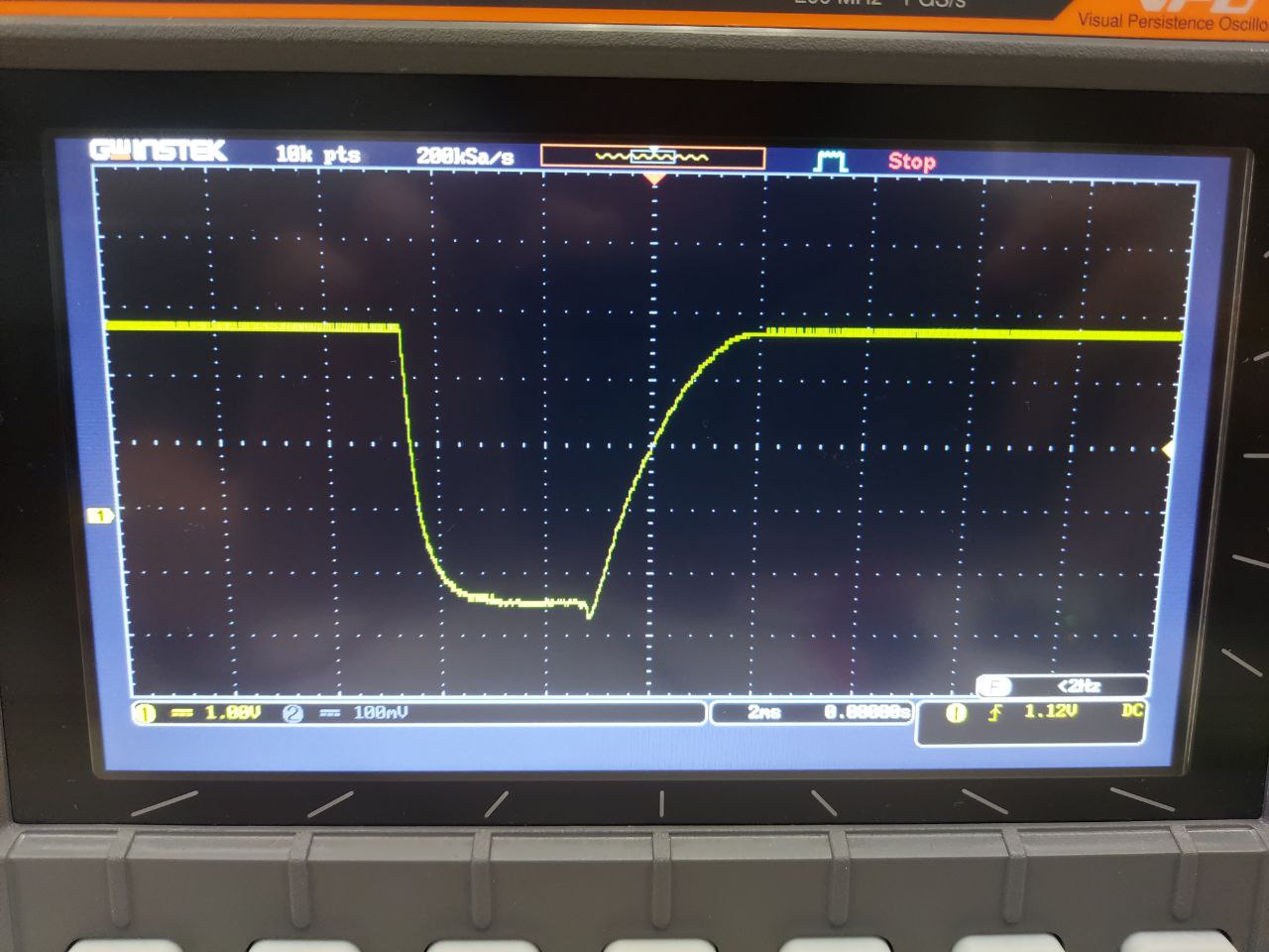
Fig 2-20 Filtered Signal
Capacitor C2 was tuned to ensure that the lowpass filter on the signal net filtered only the noise and retained a clean wave with one positive and one negative edge per signal. It is also important to ensure that the filtered signal does not a slow rise time to avoid two consecutive signals getting detected as one. The optimal value for C2 was found to be 4.7uF.
2.5 High-Voltage PCB Assembly
The assembled high-voltage PCB is as follows:

Fig 2-21 Final assembled PCB, front
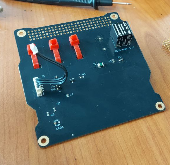
Fig 2-22 Final assembled PCB, back
2.6 Results and Verifications
2.6.1. Pre-integration Testing
After finalising and tuning the PCB, it was tested to check if it remained within project requirements defined at the start of the project.
GM Tube Operation Test
A blue LED, LED1, was temporarily soldered on the PCB in the location displayed on figure 18. If a particle was detected, the resultant signal pulls the signal net low and current flows through the LED, turning it on briefly. Once the signal passes, the net will be pulled high again and the LED turns off as no current flows through it. Hence, an LED blink indicates one signal pulse. The PCB was connected to the oscilloscope which displayed the pulses on the signal line. The time scale of the oscilloscope was set to 500ms to display all pulses within 5 seconds on the entire screen. An Arduino Uno was programmed to record and print its signal counts every 5 seconds.
Fig 2-24 Testing setup with synchronised microcontroller counts, oscilloscope pulses and LED blinks
The LED blinks whenever a new pulse appears on the oscilloscope screen, and it blinks the same number of times in 5 seconds as the number of pulses present on the oscilloscope screen. The microcontroller’s counts is also synchronised with the number of pulses on the screen. Hence, the microcontroller is accurately recording pulses from the GM tube.
Current Consumption
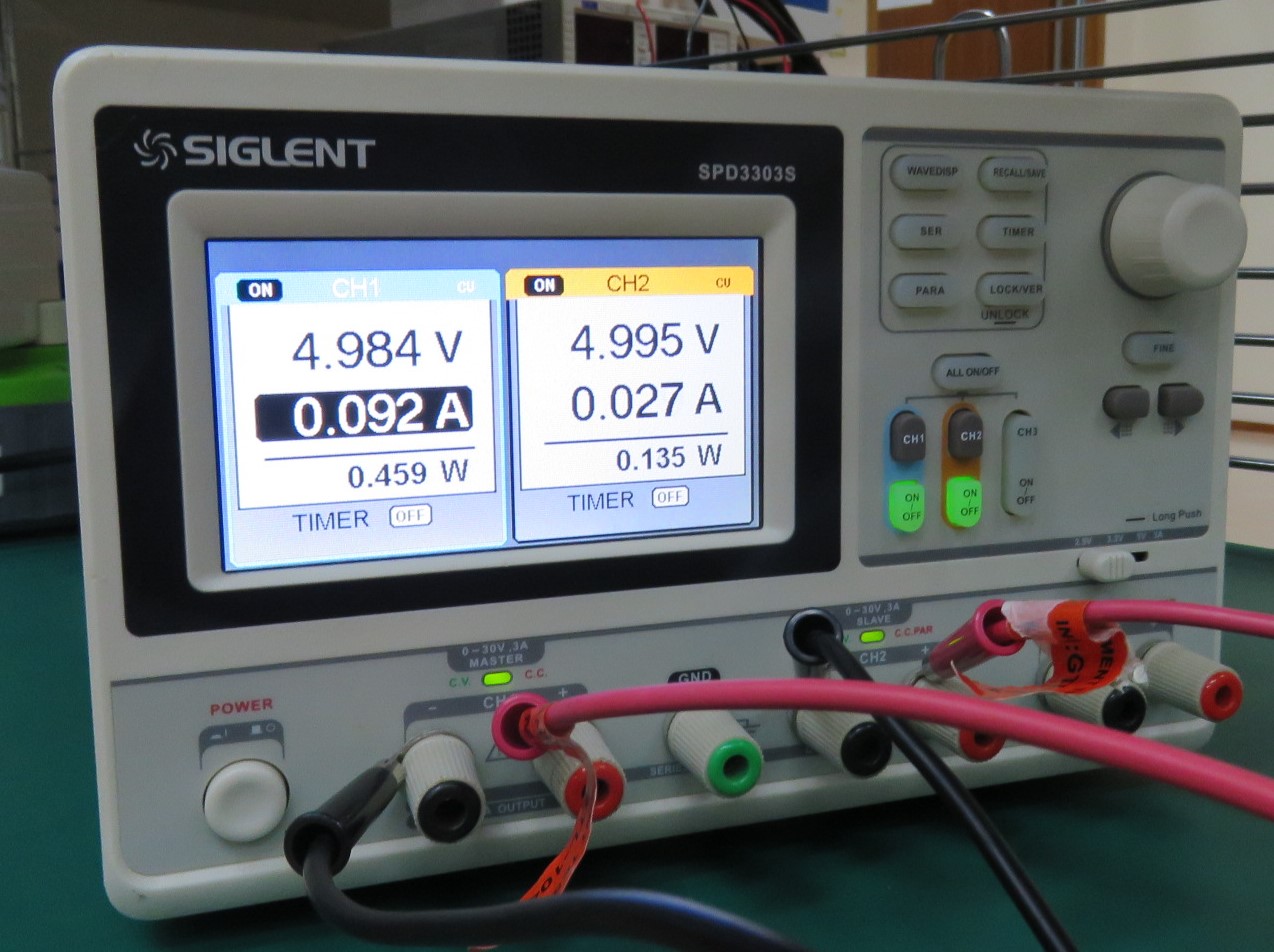
Fig 2-25 Current drawn by the high-voltage PCB (left) and the low-voltage PCB (right)
The high voltage PCB consumed between 0.086A to 0.14A. The high-voltage PCB, combined with the current drawn by the low-voltage PCB of between 0.026A to 0.032A, will draw a maximum current of 0.172A. This is lower than the 2A limit for our payload. Hence the 2A current supply limit is satisfied.
Maximum Temperature during Operation
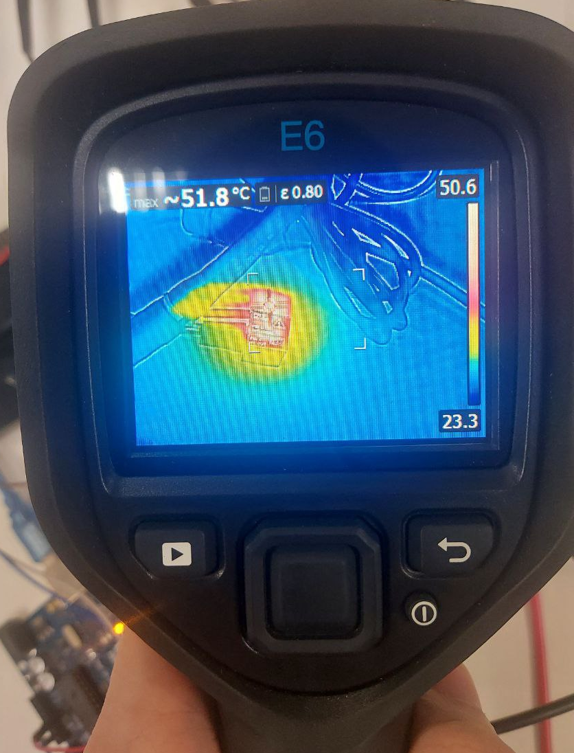
Fig 2-26 Thermal imaging of the circuit, converter is the hostess component
After running for 4 hours, the hottest component on the PCB was found to be the converter, and its temperature plateaued at 51.8°C degrees Celsius. As the maximum temperature reached by the converter is within its recommended operating temperature of -25°C to 70°C (Advanced Energy, 2023), the converter should be able to operate for prolonged periods of time during the mission.
2.6.2 Qualifications Testing (Post-integration)
The high-voltage PCB is then integrated together into the rest of the payload and sent for qualification testing. Vibration and thermal cycle tests were conducted on the payload in the ST Engineering Advanced Networks and Sensors facility.
Sine and Random Vibration testing
The payload underwent both sine vibration and random vibration testing in all three axes to tet for its mechanical stability. The specifics of the sine and random vibration test will be elaborated in Mingchuan’s section.
After the vibration testing, the payload was retested for any damage. It is found that the GM tube can still provide counts per minute in the appropriate 5 to 60 range (ECOTEST, 2025), showing that the high-voltage PCB and its components is undamaged. This proves that the components chosen for the high-voltage PCB can withstand the intense vibrations during launch.
Thermal Testing
The payload was then subjected to 16 hour thermal cycle testing, with 4 hours each in cold (-25°C) and hot (+70°C) phase. The GM tube’s counts per minute are then collected over this time and plotted along the temperature.
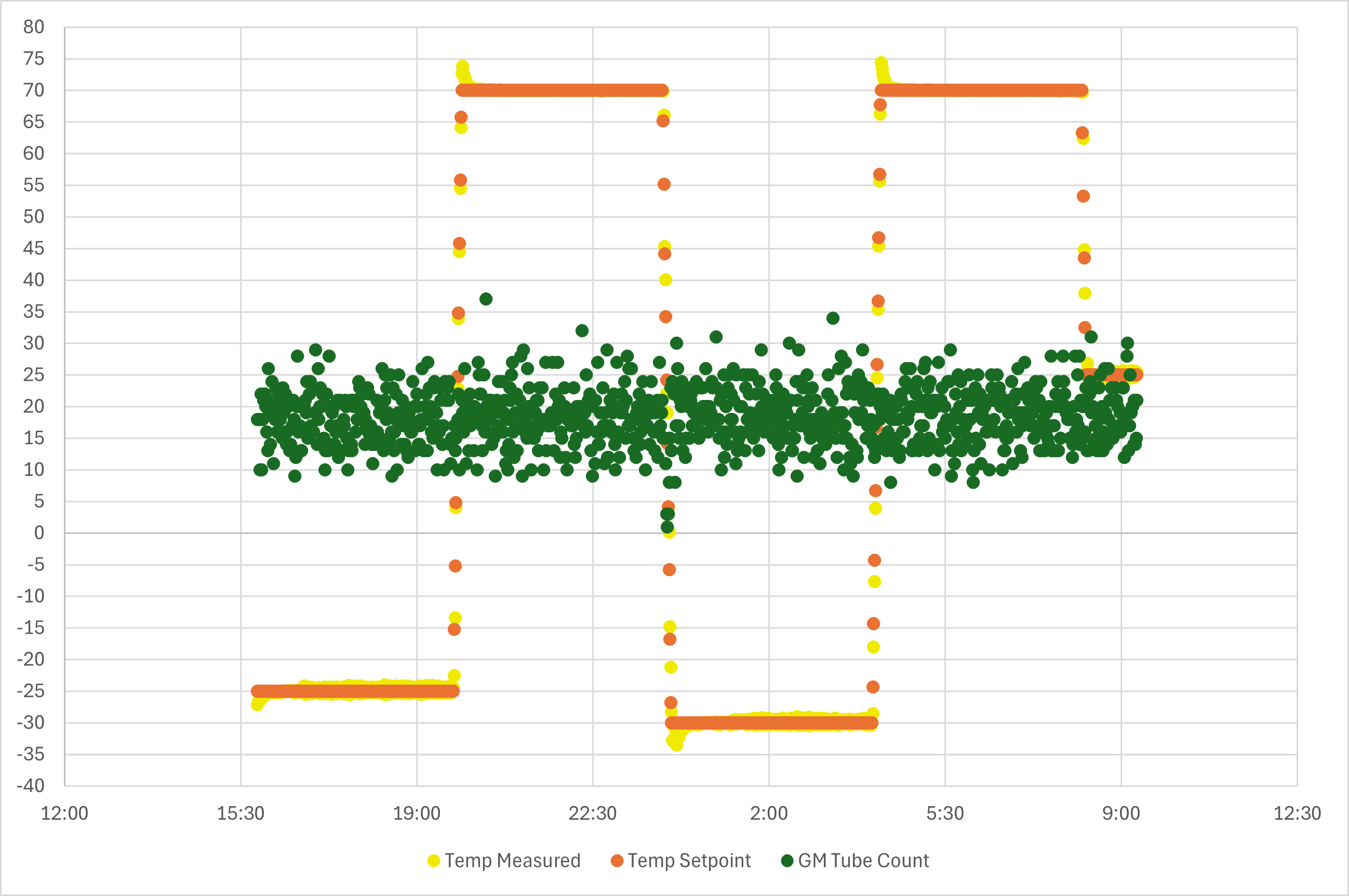
Fig 2-27 Plotting counts and temperature across duration of thermal cycling
The PCB generally operated as per normal, detecting between the normal range of 5 to 60 counts per minute (ECOTEST, 2025), indicating no substantial damage to the circuit and proving its reliability over a wide temperature range that it is expected to experience in space.
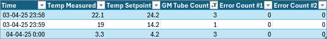
Fig 2-28 Outlier Count Data
Upon closer analysis, the count was unusually lower than 5 counts per minute for three minutes, at around 12 midnight. This may be due to a momentary event where the converter supplied less than the minimum voltage range of 450V to the GM tube. If the GM tube does not receive enough voltage, its signals will have a shorter period and get filtered by the lowpass filter on the signal net. Hence the detected signals may not be recorded by the ZSOM-M01.
However, the counts returned to normal immediately after, signifying that the circuit did not suffer any permanent damage. Furthermore, while this event may be attributed to the rapid change in temperature, it only occured once out of the 4 temperature shifts. Moreover, over 16 hours of testing, this event only occured once over a short 3 consecutive minutes. Hence, these 3 data points can be considered as outliers and confidence remains high in the high-voltage PCB’s ability to provide robust radiation detection under extreme temperatures and changes in temperature.
2.7 Conclusion
In conclusion, the high-voltage PCB have successfully proven that it can provide reliable radiation level readings even under extreme temperature environments and remains undamaged under intense vibrations. Furthermore, the additional materials like cable tie and thermal pad posed no outgassing issues that may interfere with the other components and payloads.
2.8 Future work
Moving on from our current stage, more development can be done in the lead up to launching our payload:
- Further testing and development on GM tube circuit to further prevent outlier data as seen in the thermal cycling test.
- Noise can be filtered from the 5V and 3.3V Picoblade input to further prevent noise from generating false counts.
- Optimise the thermal pad more to ensure higher heat transfer from the converter to the shielding.
- Assemble the final flight model and send it for protoflight testing.