
Sowmya Srinivasan
Year 4 Electrical Engineering
A0246190H
3. The Bit Flip Experiment
3.1 Objectives, Scope of Work & Deliverables
Objective: The design and implementation of the Radiation-SEU Correlation experiment.
Final Deliverables:
- Design of the experiment
- A space-grade implementation of the design
- Integration with the rest of the payload
3.2 Problem Context and Value Proposition
3.2.1 Problem Context
Bits that represent either data or programs are stored in computer memory as charge. Ionized particle radiation can alter this charge and cause bit flips that corrupt data. This is called Single Event Upsets (Baraniuk, 2022). Without sufficient data on SEU, it is hard to create solutions that safeguard the processors in space.
3.2.2 Identification of Research Gap
The image below depicts the current state of data and experiments on bit flips. Further details on the experiments pertaining to microcontrollers can be found in Appendix C.1. But the diagram below highlights the gap.
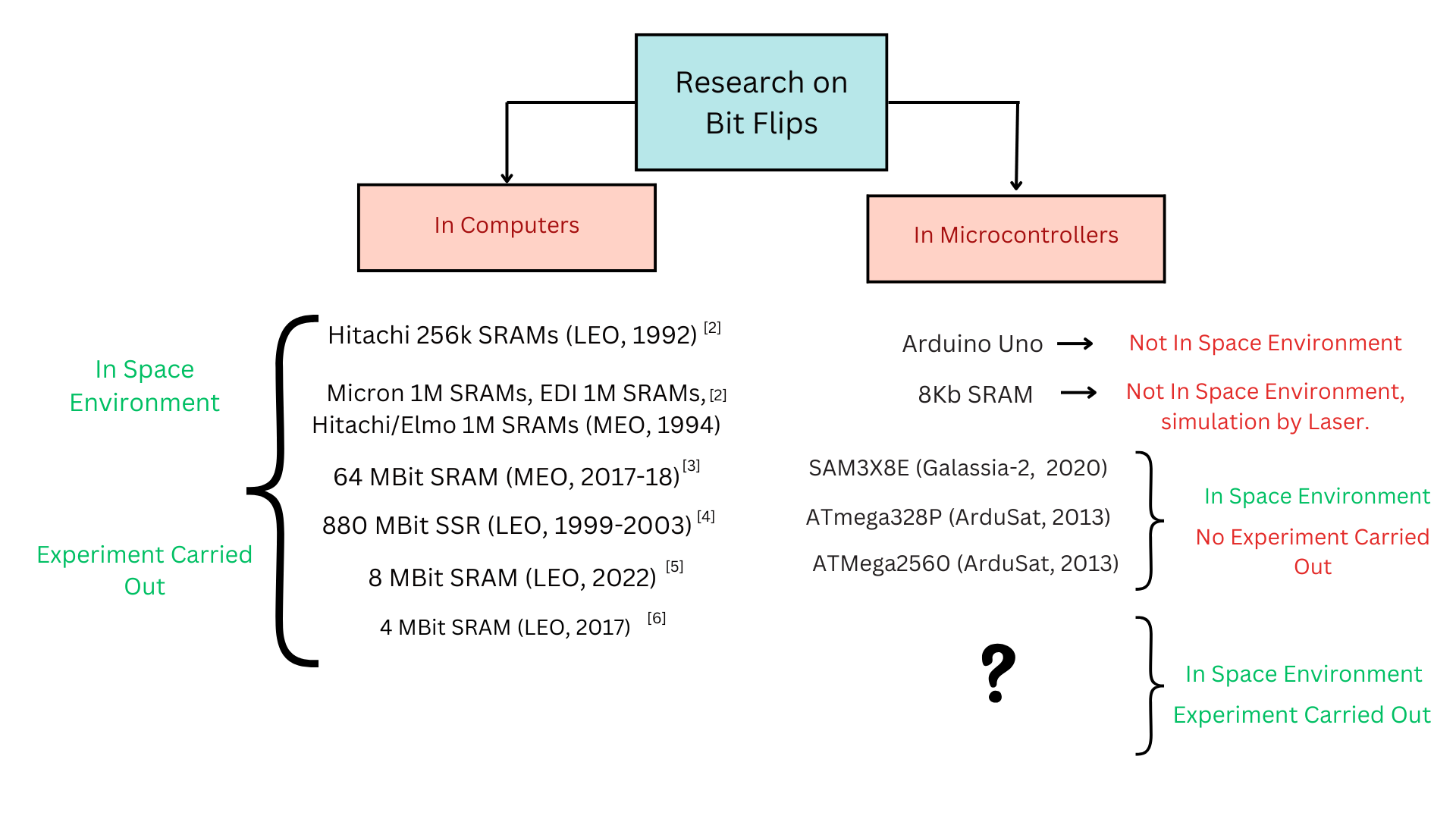
Fig 3-1 Existing State of Research on Bit Flips
Reference Keys: [1,2] (Seidleck, 2002) [3] (Noeldeke, 2021) [4] (Poivey) [5] (Coronetti, 2024) [6] (Brian D. Sierawski) [7] (Olsen, W.) [8] (Wang, 2022)
While there are many studies on larger SRAM sizes, there is a Lack of data on Microcontroller Bit Flips in LEO in comparison with Radiation Counts.
3.2.3 Value Proposition
CubeSats, which are becoming increasingly popular, extensively use microcontrollers and operate in LEO. While data about larger SRAMs can provide developers with a rough idea of what to expect, it cannot be confidently applied to microcontrollers. Hence, this experiment bridges the gap by collecting microcontroller bit flip data in LEO to benefit CubeSat developers and carrier services.
3.3 Design Overview
3.3.1 Concept of Experiment
Two microcontrollers of the exact kind will be placed in the payload, with only one of them shielded (according to Mingchuan’s section). Their SRAM data will be periodically requested every minute by the payload’s central processor. Their error counts are then computed and stored, along with a 10 percent sample of the SRAM.
On Earth, this error count can be compared with the radiation counts from the on-board GM Tube (from Weihao’s section) in order to derive a correlation between counts of certain types of radiation and bit flips. In addition, we can also compare the error counts in order to understand the effectiveness of the shielding method. As a collateral, we also understand the radiation tolerance of the microcontroller under test.
For a more detailed/specific explanation of the concept and possible inferences please refer to Appendix C.2.
3.3.2 Design Specifications
The design was constrained by the following specifications.
| Feature | Specification | Reasoning |
|---|---|---|
| Current Consumption | <100mA | The central microcontroller (ZSOM) is rated for 500mA, including its own operation. It is reasonable that the experiment should draw <20% of the total current resource. |
| Operating Voltage | 3.3V | The ZSOM supplies power at 3.3V, and has logic voltage of 3.3V as well. |
| Duration of Data Transfer | <12s | The experiment is to be conducted every minute. Since other tasks need to be done in that time, only <20% of the time should go for data transfers. |
| Size of Experiment Payload | <4088 mm² in Area, but can be double sided. <20mm height on inner side <3mm height on outer side | Derived from payload dimensions, shielding presence and layout. Data present in [Appendix E.11](/cde4301-final-report/appendix-e/#appendix-e11-usable-area-of-pcb-and-size-of-components) |
| Minimum Size of Memory to count bit flips | > 1 Kb | According to (Matthews, M., 2021) up to 10 upsets can happen over 1kB per day. <1 kB means too little information from the experiment. |
| Maximum Size of Memory to count bit flips | ≤2.56Kb | Restricted by the data budget of only 256 bytes per microcontroller. A minimum sampling of at least 10% is desired for good data collection. |
Table 3-2 Design Specifications Table
3.3.3 Design Choices Summary
| Requirement | Component Choice | Reasons |
|---|---|---|
| Microprocessor Chip For Experiment | ATMega32U4 | - Has SRAM of suitable size and has I2C. - Likely to be used in future space applications due to built-in USB support. |
| Area to Observe Bit Flips | SRAM | - Very high susceptibility to bit flips. - Easy to read and reset. |
| ATMega to ZSOM Communication | I2C Protocol | - Supports multiple devices connected to the same bus. - The only such available-to-use interface on ZSOM. |
| I2C Robustness Method | Bus Reset and Power Cycling | -Bus reset makes the slave release the SCL line, which is often the reason for lock-ups -Power cycling resets the ATMega32u4, if the error is due to other reasons |
| Bus Reset Implementation | 9 Pulses on SCL after Timeout | -Standard method for lock-ups caused by SCL pulled low is to toggle 8-16 times (Nguyen, D.) |
| Power Cycling Implementation | PMOS Switch x 2 | -Pulls up completely to 3.3V -Low static power consumption -Separate PMOS for each ATMega32U4 to support graceful degradation if needed |
| Power Source of ATMegas | ZSOM SEL protected 3.3V line | -Provides latch-up protection to ATMega32u4s -Supplies more than sufficient current |
| Bootloader | Caterina by SparkFun | -Supports 8MHz 3.3V operation and D+D- programming -In use by Sparkfun Pro Micro boards |
| Bootloader Upload Method | ICSP using avrdude | -Popular and reliable method |
| Program Upload Method | D+ D- Inbuilt USB | -Suggested method for ATMega32u4 & Caterina bootloader |
| Reference Microcontroller Board | SparkFun Pro Micro 3.3V, 8MHz | -Uses the same chip, frequency and voltage as requirements -Trusted source |
Table 3-3 Design Choices Summary Table
The above table only summarizes the final choices. Detailed reasons for the selections consisting of comparison tables of alternative solutions and addressing I2C related concerns were covered in the Interim and are also present in the Appendix Section C.3 and C.4 respectively.
3.3.4 Design Overview Diagram
The below diagram represents the architecture of the experiment.

Fig 3-4 Design Overview
3.4 Design Details
3.4.1 Schematic Entry for PCB
Link to download and view the schematic is available at Link.
Link to download and view the board is available at Link.
ATMega32U4 and supporting circuitry
- Circuit was fully referenced based on the SparkFun Pro Micro Schematic Link.
- Only the load capacitor for the crystal oscillator was changed to suit the selected oscillator, which is about 18pF according to the datasheet.
- Since the microcontroller is running only at 8MHz, there is a decent margin to alter the crystal oscillator load capacitances.
- This circuit was verified by Prototype #2 (PCB)
I2C connections
- Standard bus configuration with pull-up was used.
- The 3.3V on the ZSOM (without latch-up) protection supplies the pull-up since it needs to be a permanent pull-up.
- Pull-up resistors were chosen to be 4.7k ohms, which is popular in microcontroller-based I2C design.
- This circuit was verified by Prototype #1 (Table-Top)
CAN Transceiver module
- The CAN module essentially converts SPI of ZSOM-M01 to CAN signals.
- Design was referenced based on a SPI to CAN breakout board we tested with Link.
- However, it was adapted to work at 3.3V by changing TJA1050 to TCAN334RD.
- The oscillator and corresponding capacitors were altered as well to be the same as that for ATMega32u4 circuitry.
Power Cycling circuit
- A simple PMOS switch was implemented.
- Decision to leave out the usually present BJT was based on trial and error, which showed that current consumption and sensitivity to resistance (hence temperature) values is greater in the case of BJTs.
- Each ATMega32u4 is controlled by a separate PMOS switch for graceful degradation. This is done in case the unshielded chip gets severely damaged and corrupts the bus. With a separate PMOS, we can disable the noisy chip and at least collect data from the shielded ATMega32u4.
PCB Traces
- The CAN lines, which are a differential pair, were routed with symmetry and consistent spacing as much as possible, as advised by Altium Resource.
- For the I2C lines, the guideline of spacing to be at least 3 times the width of the lines, according to the above article, has been followed.
- There is a polygon pour ground plane across the PCB to reduce noise.
- On the conservative side, 0.254mm traces were used for signal routing and 0.4064mm traces were used for 3V3 and 5V lines. This was done by using the PC104 or Pico Blade specification of maximum 1A per pin as a clear upper limit. This complies with the recommendations in Altium Resource.
3.4.2 Chip Programming
Programming Steps
- The Caterina bootloader was flashed onto the chip through ICSP using a SparkFun Pro Micro as the ISP. The tool used for this was avrdude.
- The Low fuse was ensured to be 0xFF to be able to use an external oscillator.
- After this, the application program was flashed onto the chips using ArduinoIDE via the D+ D- pins over a USB connection.
The code used for the ATMega32U4s (slaves) and ZSOM’s (master) I2C can be found in Appendix C.5.
3.4.3 Current Budget Table
In the table below, a conservative estimate of total current draw by the experiment setup was done by considering operation currents for the key chips involved in the design.
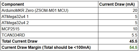
Table 3-5 Current Budget Table
Apart from this, other components would also draw some power, so we can round up this estimate to 50mA. To estimate a rough power requirement, we can take 5V as the operating voltage to obtain, Power Consumption Estimate = 0.25W
3.4.4 Bill Of Materials & Temperature Tolerance Table
| S. No | Component Name | Temperature Range (C) | Material / Description | Item No with Link |
|---|---|---|---|---|
| 1 | Crystal Oscillator | -40 to 85 | Hermetically Sealed with Glass | ABM3-8.000MHz-D2Y |
| 2 | 18pF Capacitor | -55 to 125 | Cu, Ni, Sn, C0G | GJM1555C1H180GB01 |
| 3 | 1uF Capacitor | -55 to 125 | Cu, Ni, Sn, X7R | CL10B105KP8NNNC |
| 4 | 0.1uF Capacitor | -55 to 85 | Cu, Ni, Sn, X7R | CL05B104KP5NNNC |
| 5 | 10uF Capacitor | -55 to 125 | Cu, Ni, Sn, X7R | GRM21BR61C106KE15K |
| 6 | 10kohm Resistor | -55 to 155 | Thick Film Resistor | RC0402FR-7W10KL |
| 7 | 4.7kohm Resistor | -55 to 155 | Thick Film Resistor | RC0402JR-074K7L |
| 8 | 120ohm Resistor | -55 to 155 | Thick Film Resistor | RC1206FR-07120RL |
| 9 | 22ohm Resistor | -55 to 155 | Thick Film Resistor | ERJ-2RKF22R0X |
| 10 | ATMega32U4 | -40 to 85 | COTS chip | ATMEGA32U4-AU |
| 11 | PMOS AO3401A | -55 to 150 | COTS PMOS | AO3401A |
| 12 | MCP2515 | -40 to 125 | COTS chip | MCP2515-E/SO |
| 13 | TCAN334DR | -40 to 125 | COTS chip | TCAN334DR |
| 14 | Picoblade Connectors | -40 to 105 | Widely used in Cubesats | 532610671 |
| 15 | Picoblade Wire | -40 to 105 | Widely used in Cubesats | 15134-0600 |
Table 3-6 Bill of Materials & Temperature Tolerance Tables
Overall,
- All the components meet the (-30, 70) degrees C range needed for Qualification.
- The materials involved are acceptable because this payload is for a Cubesat, which often uses COTS components.
- There is space heritage for the thick film resistors, X7R/C0G capacitors, and Picoblade connectors in Galassia-1 and Galassia-2.
3.4 Prototyping Overview
Images of prototyping iterations and final product can be found in Appendix C.6.
3.4.1 Prototype 1
Description: Table top Setup to Test Functionality
Objectives:
- To obtain realistic values for current consumptions, data transfer time
- To verify bootloader and code flashing, SRAM dumps, I2C setup, Power Cycle & Bus Reset Implementation, and Repeatability
Approach: The below table describes how each aspect was implemented in the prototype.
| Feature | Implementation in Prototype |
|---|---|
| Central Microcontroller | SparkFun Pro Micro 3.3V, 8MHz |
| MCUs under test | 2 x SparkFun Pro Micro 3.3V, 8MHz |
| PMOS Switch | SMD PMOS soldered onto veroboard + wires |
| I2C Bus | On the breadboard + wires |
Table 3-7 Table Top Setup
Outcome
- All the functionality was verified and possible.
- Overall Current Consumption was 33mA (within specification <100mA).
- Overall time for 1 run of experiment was 10.3 seconds (within specification <12s).
3.4.2 Prototype 2
Description: A functional PCB implementation, but without CAN, only 1 PMOS, and dimensionally inaccurate
Objectives: To have a functional PCB and identify any fundamental issues in operation
Approach: Since the purpose was only to test functionality on PCB, a rough dimension PCB of 10x10cm was made.
Outcome:
- The PCB was fully functional in terms of desired features.
- Current Draw was in the range of 0.028 to 0.031 mA.
- Overall Time for one run of the experiment was 10s.
Actionables:
- Realization that it is better to have 2 PMOS so that only the faulty one can be disabled.
- Realization that all components need to have a wide enough temperature range with sufficient margin.
3.4.3 Prototype 3
Description: A functionally and dimensionally accurate PCB Implementation with CAN, 2 PMOS and dimensionally accurate
Objectives: To test if integration with Central Code (Richard), HV PCB (Weihao) and Mechanical (MingChuan) was possible and functional.
Approach: The PCB was resized, CAN was added, a second PMOS was added. After this we checked mechanical fit with the shielding manufactured, as well as overall integrated functionality.
Outcome:
- The whole payload could be integrated and function as one with all desired functionality.
- Realization that the temperature range of the oscillator does not provide enough margin.
Actionables: For the final product, the only change made was to select an oscillator with as wide a margin as possible to be on the safer side, since I2C needs an accurate clock that shouldn’t be affected too much by extreme temperatures.
3.5 Final Product Testing & Results and Evaluation
3.5.1 Basic Tests & Evaluation
The below table lists the basic verifications carried out on the experiment PCB.
| Test For | Method | Outcomes |
|---|---|---|
| Intact Connections and No Shorts | Multimeter on Continuity Mode | All necessary connections were connected to each other. All non-connections remained disconnected. So, the board was electrically functional in the same way as the design. |
| Functionality of the PCB and Code | Different variations of SRAM bit pattern were stored into the ATMega32u4s and SRAM dumps were examined. Bus lock-up was simulated (Error cases elaborated in [Appendix C.4.2](/cde4301-final-report/appendix-c/#c42-error-case-vs-code-element-that-handles-it)) and Bus Reset and Power Cycling was carried out. | The chips on the PCB were able to be reprogrammed with different codes. They always gave the correct SRAM dump output. Bus lock-up detection, Bus Reset and Power Cycling were all successful. So, the PCB design has all the desired functionality. |
| Time for Transfer | After integration, a test run was carried out to see if the system can complete all necessary operations every minute. | The integrated system had sufficient time to complete all necessary operations per minute. So the experiment setup occupied an acceptable amount of time. |
| Current Draw Limit | Power draw was tested using Lab Bench Supply | The maximum current draw ever observed for the experiment PCB is 32 mA. The current usually varies in the range 26mA - 32 mA. The voltage supplied was at 4.997V. Hence the total current draw is <100mA and meets the constraint. |
Table 3-8 Basic Tests and Evaluation
3.5.2 Space Related Tests & Evaluation
In order to test the functionality of the product and understand aspects of its endurance in space and also during launch, we carried out the following tests at ST Engineering’s Jalan Boon Lay Facility.
Thermal Cycle Test: A 16 hour long test, comprising 2 thermal cycles. Each cycle consisted of 4 hours at -30 C, followed by 4 hours at 70 C. To simulate the temperature fluctuation in space.
Switch-on Test: Tested for both -30 C and 70 C. For this test, the payload was kept at the first extreme temperature, -30 C for an hour, after which it was switched on and operated at -30 C for another hour. The same was done for 70 C
Vibration Test: A sine and random vibration test was carried out to understand its mechanical durability (further elaborated in Mingchuan’s Section).
The below table explains the testing goals, method and outcomes for the final product.
| Test For | Method | Outcome & Inference |
|---|---|---|
| Repeatability and Endurance | The payload was kept running continuously for 16 hours. | The experiment setup can endure at least 960 continuous SRAM reads. So, it is beyond suitable to carry out the 60 continuous reads needed during the experiment. |
| Correctness of Data Transfer Across Temperature Extremes | The payload was subjected to the 16 hour thermal cycle test mentioned above. | The plot of error count versus temperature shows that the SRAM data is correctly transferred for long periods of time, and under harsh temperatures (-30 to 70 C). This indicates that the experiment setup is robust to the temperature variation it will experience in space during operation. |
| Ability to Switch on at Temperature Extremes | The payload was subjected to the Switch on Test, described above. | The payload was able to switch on and operate at the temperature extremes of -30 and +70 C. This means the experiment start-up is robust to the temperature variation it will experience in space. |
| Mechanical Strength | The payload was subjected to the vibration testing described above. | The payload was operational after being subjected to these tests, and also visually appeared to be intact. This implies that the solder joints in the design are of sufficient strength and further reinforcement is not required for vibrations of the tested frequencies - which are the expected frequencies during launch. |
Table 3-9 Space Related Tests and Evaluation
The below image shows that the error counts for both SRAMS are consistently zero over the entire range of temperature variation. Hence, the product is reliable under these conditions.
Please note that the Error counts from both SRAMs are the same hence only the pink line shows in the graph.
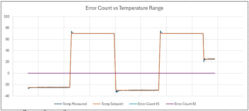
Graph 3-10 Graph for Error Counts vs Temperature Variance
3.6 Future Recommendations
3.6.1 Steps Towards Launch
- Proceed to Proto-flight test and ensure everything operates properly.
- Find a launch partner and coordinate the interfacing between PCB pinout and their satellite.
3.6.2 Future Design Recommendations
- If more area is available, or in a second version of this mission, use different MCUs and derive a correlation between similar families of MCUs when it comes to radiation tolerance.
- If a higher data budget is available on OBC, take full SRAM samples at a lower rate to understand the exact spatial correlation of errors.
3.7 Conclusion
The Radiation-SEU Correlation experiment has been fully designed and implemented, including a space-grade version integrated with the rest of the payload. Extensive testing has verified its functionality under some harsh space and launch conditions.
During the payload’s spaceflight, the experiment will provide data on bit flips in microcontrollers relative to radiation counts, along with insights into the impact of the shielding under test.
This data will help CubeSat developers better understand and address the effects of space radiation on microcontrollers in Low Earth Orbit, significantly aiding future projects by providing a foundation for evaluating cost-effective and simpler solutions for managing Single Event Upsets.