Appendix C
Appendix C.1 Details on Bit Flip Experiments on Microcontrollers in LEO
C.1.1 Olsen, W., Wood, B., & Dennison, J. (n.d.). Microcontroller Survivability in Space Conditions.
- This experiment focused on an Arduino Uno’s ability to function properly inside the Materials Physics Group’s (MPG’s) Space Survivability Test (SST) Chamber.
- The Chamber holds vacuum and contains a Sr90 beta radiation source with a dose rate of 0.1 krad/hr at a 30 cm distance over a 15 cm diameter sample area.
- The dose rate was only important as it related to the total ionizing dose (TID). This enabled closer placement of the Arduino to the source, increasing the TID rate to ~0.991 krad/hr.
- A program was used to monitor for soft errors as well as permanent failures.
- The conclusions made were:
- The program did not show any failures even though the TID was well into the MEO range.
- There was an error during code re-upload that could be due to damaged bytes in the SRAM or flash memory.
C.1.2 Wang, X., Chen, R., Yuan, R., Chen, Q., Liang, Y., & Han, J. (2022). Experimental Study on the Space Electrostatic Discharge Effect and the Single Event Effect of SRAM Devices for Satellites.
- The study used two types of simulations to examine the effects of space environments on SRAM devices:
- Space Electrostatic Discharge (SESD): This was simulated using an ESD (Electrostatic Discharge) generator.
- Single Event Effect (SEE): Simulated using a pulsed laser to mimic space radiation effects.
- Device Tested: A low-power, asynchronous SRAM device was selected for the study.
- Conclusions:
- The Single Event Upsets (SEUs) caused primarily single-bit errors in the SRAM device.
- The error rate of SEE-induced errors increased with the intensity of the laser pulses.
Appendix C.2 Detailed Concept of Experiment & Possible Inferences
C.2.1 Basic Idea
- The experiment comprises 2 microcontrollers of the same kind being sent to space, one shielded and one unshielded.
- While having multiple microcontrollers with different shielding materials or thickness would be ideal, the space constraint and data budget limit permit only 2 microcontrollers to be used.
- Hence, one microcontroller is unshielded, while the other is shielded (shielding is from Mingchuan).
- Both the microcontrollers under experiment would experience bit flips, and every minute, a central microcontroller (selected by WeiHao) gathers the data on bit flips from them. The reasoning for a 1 minute interval is in Appendix C.2.3
- The central microcontroller then computes the error count by comparing the fixed pattern with the received pattern and also stores either error indices or a 10% sample of the SRAM to memory. (information to be stored is decided by Richard)
- The radiation counts per minute is measured by a Geiger Muller tube (selected by Wei Hao). Exactly what kinds of radiation is counter is in Appendix C.2.4
C.2.2 Possible Inferences From Experiment Data
- The error count of the unshielded microcontroller would tell us the extent of radiation tolerance of the chosen MCU.
- Comparing the error count of the unshielded microcontroller with the Radiation CPM of the Geiger Tube would allow us to quantify the correlation between SEU and particle radiation in LEO.
- Comparing error counts of the shielded and unshielded microcontrollers would quantify the effectiveness of the shielding method.
C.2.3 Reasons for 1 Minute Intervals between Samples
- Given that a LEO takes 90-120 minutes, we would want to conduct the experiment for at least half the orbit duration. Since the rideshare is not decided upon, we go with the higher number of 60 minutes per orbit.
- A finer resolution in time is preferred in general, to prevent double bit flips from occurring since our bit flip count cannot reflect double flips.
- However, the data budget shows that we can run up to 60 runs of the experiment per orbit. Hence, the interval between runs is decided as 1 minute.
C.2.4 Specificity about the Radiation Particles
The exact correlations we’ll be able to derive is only between the particles the Geiger-Muller Tube can detect and the Bit Flips. For specificity sake, the following are the particles we can evaluate correlation for: Alpha Particles + Beta Particles + Gamma Rays.
Appendix C.3 Detailed Evaluation and Selection of Potential Solutions
C.3.1 Ideal Cases, Comparison Tables and Final Selection
For each aspect of the experiment, a design choice had to be made, as elaborated below.
The Memory Device
The Ideal Case: Easy to read, Highly susceptible to bit flips, Size of 1 to 2.56 kB, Easy to reset, does not lose data upon power cycle due to SEL .
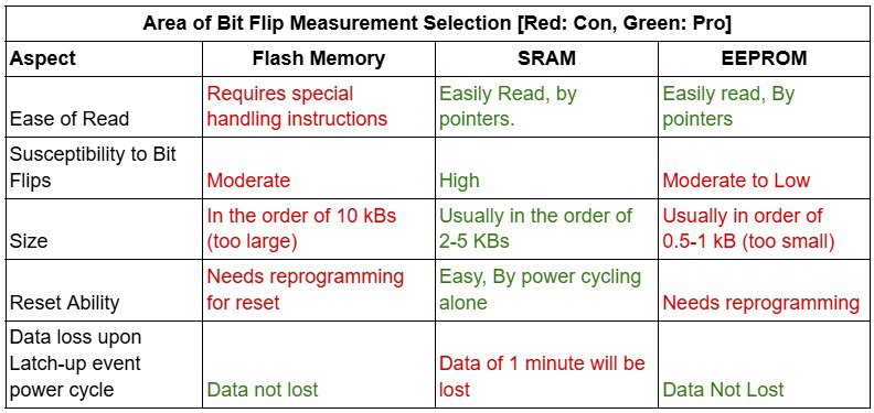
Table C-1 Selection of Memory Device
Due to the highest number of positives, the SRAM was chosen as the memory device. The one drawback, that is of data loss upon occasional latch-up events, is deemed to be worth the benefit of a simpler reset, which will be needed more often than the latch-up events.
ZSOM to Microcontroller Communication
The below table lists the communication peripherals on the ZSOM board and its availability or relevance for this experiment.
| Communication Interface | Can it be used for this experiment? |
|---|---|
| SPI | No. SPI of the ZSOM is being used to implement CAN protocol and interface with the OBC, which shouldn’t be interfered with. |
| UART | No. UART is a peer-to-peer protocol. The experiment needs a bus protocol for 2 ATMegas to communicate to the ZSOM. |
| I2C | Yes. It is not being used for any other purpose and is a bus protocol. Also, data transfer speed is sufficient. |
Table C-2 Selection of Communication Interface
Due to I2C being the only interface on the ZSOM that is available for use and supports multiple devices, I2C is chosen as the communication interface between the ZSOM and the ATMegas.
Since it is known that I2C can face problems in the space environment, the experiment incorporates a timeout feature followed by bus reset and/or power cycling to provide robustness to the transfer of data.
Further elaboration on the various issues faced by I2C and our approach towards managing it elaborated on in Appendix Section C.4
The Microprocessor
The Ideal Case: Has I2C Interface, a readable SRAM, NO flight heritage, SRAM in 1-2.56 kB size range, high probability of use in future missions
After applying an initial filter of SRAM sizes, availability of documentation, popularity, and presence of unique features, the following 3 microprocessors were shortlisted for a good demonstration of the reasons for selection.
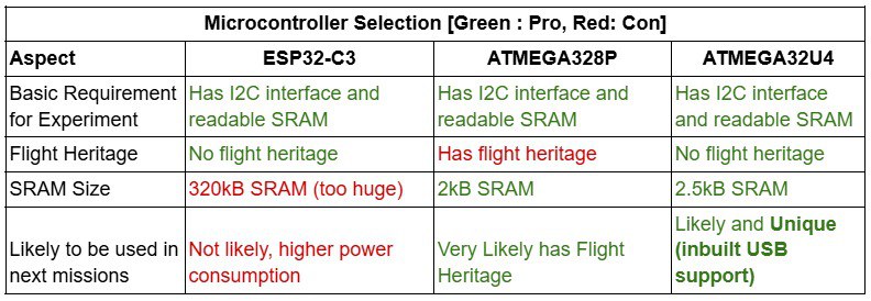
Table C-3 Selection of Microprocessor
Hence, ATMega32U4, having the most positives, is selected as the Microcontroller under experiment.
The next sections of the appendix further elaborates on
- The reasoning towards not selecting other microcontrollers with USB support (Appendix C.3.2)
- Explanation of the flight heritage relevance of the ATMega328P (Appendix C.3.3)
Other Components
| Component | Choice | Reasons |
|---|---|---|
| Power Source for ATMegas | 3.3V from ZSOM, with SEL protection | The ZSOM provides protection against latch up events so that the microcontrollers do not suffer permanent damage. ZSOM has a power cycle implementation after latch-up detection. |
| Power Cycling Method | PMOS as a digital switch | Simple and known implementation. Provides digital control. Can meet the current and voltage specifications. |
| Bootloader | Caterina by Sparkfun | Supports 3.3V and 8MHz Clock. Supports programming by D+ D- pins. In use by Sparkfun ProMicro. |
| Bootloader Upload | ICSP & Arduino as ISP | Very common, reliable method. |
| Program Upload | D+ D- USB | Only 2 additional pins to the ICSP header in the PCB. In use by SparkFun Pro Micro. |
Table C-4 Selection of Other Components
C.3.2 Other Microcontrollers having USB support but not selected
| SNo. | MCU | Reason |
|---|---|---|
| 1 | ATMega16U4 | 1.25KB SRAM only and less likely to be used in future missions because of small memory size |
| 2 | SAMD21 | It is the one already in Arduino M0+ in ZSOM |
| 3 | STM32F0/F1/F4 | 20KB SRAM is too big and not as popular |
| 4 | ESP32-S2 and ESP32-S3 | 320KB SRAM, too big |
| 5 | RP2040 | 264KB SRAM, too big and the coding environment is not simple - less likely to be used |
| 6 | Teensy | 64KB RAM, too big |
| 7 | PIC18F/32 Series | Not as user-friendly, not very popular - less likely to be used in future missions |
| 8 | AT32UC3 Series | Specifically designed for USB device applications - not broad enough, hence less likely to be used in future missions |
| 9 | nRF52840 | Has Bluetooth support that is not required in most Cubesat applications and also not popular - less likely to be used in future missions |
Table C-5 Built-in USB MCUs not selected with reasoning
C.3.3 Flight Heritage Information about the ATMega328P
- The ATmega328P microcontroller has flown on several CubeSats, with ArduSat-1 (2013) and ArduSat-2 (2014) being notable examples.
- Mitigation strategies included using software-based error correction and redundancy.
- The satellites operated successfully for their planned lifespans, indicating that these measures were effective for short-term missions in LEO.
- While the solar conditions of 2025 will be different (more intense) than the conditions of 2013, 2013 was also a time of solar peak.
- Our satellite is also going to be flying at LEO, for short-term, and during solar peak of Cycle 25.
We wish to send a new microcontroller to space that hasn’t flown in LEO orbit before, so that it can be tested for its radiation tolerance.
However, below is the table comparing the solar conditions, for more information.
| Parameter | 2013 (Solar Cycle 24) | 2025 (Expected, Solar Cycle 25) |
|---|---|---|
| Solar Cycle Peak Year | 2014 (April) | 2025 (July, projected) |
| Maximum Sunspot Number | 114 (weakest in 100 years) | 137–173 (below average but stronger than Cycle 24) |
| Solar Flares | Low to moderate (mostly C-class and M-class) | Moderate to high (increased likelihood of M and X-class flares) |
| Coronal Mass Ejections | Few and weak | Increased frequency and strength expected |
| Geomagnetic Storms | Minor to moderate | Moderate to strong |
| Auroras | Visible near polar regions | Potentially visible at lower latitudes |
Table C-6 Solar Conditions for Heritage MCUs
Appendix C.4 Addressing I2C Related Concerns
C.4.1 Possible Faults in I2C in Space Environment and Management Approach
| Problem | Management Method |
|---|---|
| Data Corruption | Data Corruptions during I2C Transfer will be counted as part of the Bit Flip Experiment since it pertains to the fundamental function of communication taken up by any COTS |
| Signal Integrity Issues | Intend to implement proper PCB design with controlled impedance for I2C trace and add series resistors to I2C lines to dampen reflections. |
| Power Supply Fluctuation | Surge protector, in the form of SEL protection by ZSOM. |
| Bus Lock-Up | Watchdog timers to reset the I2C bus in case of a lock-up (timeout feature). Power reset in case of a lockup that can’t be fixed by the recommended I2C reset method. |
| Cross-Talk | Using relatively slower clock speeds, that still provide reasonable data transfer timings, to reduce susceptibility to cross-talk. |
Table C-7 Possible Faults in I2C Detection and Handling
C.4.2 Error Case Vs Code Element that Handles it
| Error Case | Handling |
|---|---|
| SCL Lock Up (Always HIGH) | The response timeout section of the code will handle this. |
| SCL Lock Up (Always LOW) | The bus reset section of the code will handle this. |
| SDA Lock Up (Always HIGH) | The reply timeout section of the code will handle this. Because the start bit is indicated by the SDA high → low transition which is not possible when lockup. |
| SDA Lock Up (Always LOW) Clock Stretching by Slave | Same case as SCL lock up, clock is LOW for too long. The timeout duration will be the upper permissible limit of clock stretching by a slave. |
| Communication Bit Error due to Radiation | No handling, because this bit error will be included as part of the experiment. If we tried to handle this, we might power cycle too often for regular data collection. |
Table C-8 Error Case and Code Handling
Appendix C.5 Code
C.5.1 Slave Code
Refer to the following link to download the code: Link
//slave

#include <Wire.h>
#define no_of_bytes_stored 2048
#define SLAVE_ADDRESS 2
#define DATA_SIZE 2048 //1984 CHANGED
#define CHUNK_SIZE 32
#define HANDSHAKE_REQUEST 0x01
#define HANDSHAKE_ACK 0x06
#define READ_COMPLETE_ACK 0x09 //CHANGED
//CHANGED


volatile uint8_t byte_at_address;
volatile bool return_ack;
volatile bool handshake_completed;
volatile byte sram_array[no_of_bytes_stored]; // Buffer holding 2048 bytes of data
volatile int index = 0; // Current index to keep track of data to send
volatile uint16_t address;  //CHANGED
uint16_t START_ADDRESS;//CHANGED

// Handle received data (handshake request)
void receiveEvent(int bytes) {
  if (Wire.available()) {
    int request = Wire.read();
    if (request == HANDSHAKE_REQUEST) {
      return_ack = true;
    }
    if(request == READ_COMPLETE_ACK){ //CHANGED
      index = 0; // Reset index after all data is sent
      address = START_ADDRESS; //Reset address after all data is sent
      handshake_completed = false;
    }
  }
}

// Send requested data to master in chunks
void requestEvent() {
  if (return_ack){
     Wire.write(HANDSHAKE_ACK);
     handshake_completed = true;
     return_ack = false;
     return;
  }


  if (handshake_completed){
    for (int i = 0; i < CHUNK_SIZE; i++) {
      if (address < 0xAFF) { //CHANGED
        byte_at_address = *(byte *)address;
        Wire.write(byte_at_address); // Send the next byte
        address++;
        index++;
      } else {
        Wire.write(0x00); //CHANGED
      }
    }
  }
}

void setup() {
  //Fill data buffer with example data
  for (int i = 0; i < no_of_bytes_stored; i++){
    sram_array[i] = 0x55 + i%4; //0101 * length //TEMP CHANGE
  }
  START_ADDRESS = &sram_array[0]; //CHANGED

  address = START_ADDRESS; //set start address for first run //CHANGED
  index = 0; //start index for first run
  return_ack= false; //no handshake done at first
  handshake_completed = false;

  Wire.begin(SLAVE_ADDRESS); // Start I2C as slave
  Wire.onReceive(receiveEvent); // Register receive event handler
  Wire.onRequest(requestEvent); // Register request event handler

}

void loop() {
  // Nothing needed in the loop; actions are event-driven
}
C.5.2 Master Code
Refer to the following link to download the code: Link
//master

#include <Wire.h>

#define SLAVE1_ADDRESS 1
#define SLAVE2_ADDRESS 2

#define DATA_SIZE 2048 //CHANGED
#define ARRAY_SIZE 204 //CHANGED
#define CHUNK_SIZE 32

#define HANDSHAKE_REQUEST 0x01
#define HANDSHAKE_ACK 0x06
#define READ_COMPLETE_ACK 0x09
#define TIMEOUT_MS 4000 //CHANGED, *only read_sram() is changed apart from the constants

#define SCL_PIN SCL
#define SDA_PIN SDA

#define PCYCLE_PIN1 6 //to switch on devices, set to low, to switch off set to high
#define PCYCLE_PIN2 7
#define TRIGGER_PIN 8 //active low
#define LOW_PIN 9

#define DEBUG 1

//read result outcomes
#define READ_COMPLETE 1
#define TIMEOUT 2

int clear_bus_counter;
int handshake1;
int handshake2;
int error_count1;
int error_count2;
int read_result1;
int read_result2;
volatile uint8_t slave1_SRAM[ARRAY_SIZE];
volatile uint8_t slave2_SRAM[ARRAY_SIZE];
bool atmega1_on = 1;
bool atmega2_on = 1;


void clear_bus() {
  pinMode(SCL_PIN, INPUT_PULLUP);
  pinMode(SDA_PIN, INPUT_PULLUP);

  if (digitalRead(SDA_PIN) == LOW) { // Check if SDA is held low
    #ifdef DEBUG
      Serial.println("Bus lockup detected. Clearing...");
    #endif

    for (int i = 0; i < 9; i++) { // Toggle SCL to clear lockup
      pinMode(SCL_PIN, OUTPUT);
      digitalWrite(SCL_PIN, HIGH);
      delayMicroseconds(5);
      digitalWrite(SCL_PIN, LOW);
      delayMicroseconds(5);
    }

    // Release SCL and SDA lines after toggling
    pinMode(SCL_PIN, INPUT_PULLUP);
    pinMode(SDA_PIN, INPUT_PULLUP);

    Wire.begin();

    // Delay before resuming to allow the bus to stabilize
    delay(1000);
  }
  #ifdef DEBUG
    Serial.println("Bus clearing was attempted");
  #endif
}

void power_cycle(){
  #ifdef DEBUG
    Serial.println("Power Cycling Now");
  #endif
  digitalWrite(PCYCLE_PIN1, HIGH);
  digitalWrite(PCYCLE_PIN2, HIGH);
  delay(1000);
  if (atmega1_on){
    digitalWrite(PCYCLE_PIN1, LOW);
  }
  if (atmega2_on){
    digitalWrite(PCYCLE_PIN2, LOW);
  }
  delay(1000);
  #ifdef DEBUG
    Serial.println("Power Cycling Complete");
  #endif
}

bool perform_handshake(int slave_address) {
  unsigned long startTime = millis();

  Wire.beginTransmission(slave_address);
  Wire.write(HANDSHAKE_REQUEST); // Send handshake request
  Wire.endTransmission();
  Wire.requestFrom(slave_address, 1); // Request 1 byte for handshake acknowledgment
  delay(100);

  // Wait for acknowledgment within timeout
  while (millis() - startTime < TIMEOUT_MS) {
    if(Wire.available()){

      int ack = Wire.read();

      if (ack == HANDSHAKE_ACK) {
        return true; // Handshake successful
      }
    }
    delay(10); // Small delay before retrying
  }
  #ifdef DEBUG
    Serial.println("Handshake failed");
  #endif
  return false; // Handshake failed
}

void pretty_print(uint8_t c, int bytes_received){
  if (bytes_received%64==0){Serial.println();}
  if (c<16){Serial.print(0);}
  Serial.print(c, HEX); // Print each received byte to Serial Monitor
  Serial.print(" ");

}

int byte_error_counter(uint8_t c, int bytes_received){
  int err_count = 0;
  uint8_t reference_array[] = {0x55, 0x56, 0x57, 0x58};
  uint8_t reference_byte = reference_array[bytes_received%4];
  uint8_t mask = 0x01;
  //do a bitwise xor of reference with c. -> the matching bit locations will be zero, the unmatched locations = 1, count the number of 1's in the byte
  uint8_t xored_byte = reference_byte ^ c; //8'b 0100 1000
  for (int i = 0; i<8; i++){
    if ((xored_byte & mask) == 1) {err_count++;}
    xored_byte = xored_byte >> 1;
  }
  return err_count;
}

void printer_read_sram(long int time_taken, int total_error_count){
  Serial.println();
  Serial.print("Time taken for 1 SRAM dump, to compare and store ");
  Serial.print(time_taken);
  Serial.println(" ms");
  Serial.println("\nData reception complete.");
  Serial.print("Error Count: ");
  Serial.println(total_error_count);
  Serial.print("Now printing stores 10% array");
  for (int i=0; i<ARRAY_SIZE; i++){
    if (i%64 == 0){Serial.println();}
    Serial.print(slave1_SRAM[i], HEX);
    Serial.print(" ");
  }
  Serial.println();

}

int read_sram(int slave_address){
  //read from slave and append every 10th byte to array_slave + print on screen
  int bytes_received = 0;
  int slave_array_index = 0;
  int total_error_count = 0;
  int byte_error_count= 0;

  long int start_time = millis(); //CHANGED

  while ((bytes_received < DATA_SIZE) && (millis()-start_time <TIMEOUT_MS)){ //CHANGED , consider changing to DATA_SIZE - CHUNK SIZE + 1
    Wire.requestFrom(slave_address, CHUNK_SIZE); // Request CHUNK_SIZE bytes//keep requesting in chunks of 32 from slave.

    while (Wire.available()) { //CHANGED
      uint8_t c = Wire.read(); // Read a byte
      #ifdef DEBUG
        pretty_print(c, bytes_received); //print it
      #endif

      //CHANGED
      byte_error_count = byte_error_counter(c, bytes_received); //count number of errors
      total_error_count = total_error_count + byte_error_count; //increment error count

      if ((bytes_received%10 == 0) && (slave_array_index < ARRAY_SIZE)){ //append to array
        if (slave_address == SLAVE1_ADDRESS){slave1_SRAM[slave_array_index] = c;}
        if (slave_address == SLAVE2_ADDRESS){slave2_SRAM[slave_array_index] = c;}
        slave_array_index++;
      }

      bytes_received++;

      if (bytes_received >= DATA_SIZE) {
        Wire.beginTransmission(slave_address); //CHANGED
        Wire.write(READ_COMPLETE_ACK); // Send handshake request
        Wire.endTransmission();
        if (slave_address == SLAVE1_ADDRESS){error_count1 = total_error_count;} //set total error count
        if (slave_address == SLAVE2_ADDRESS){error_count2 = total_error_count;}
        #ifdef DEBUG
          printer_read_sram(millis()-start_time, total_error_count);
        #endif
        return READ_COMPLETE; //return
      }
    }
  }
  //else if timeout
  #ifdef DEBUG
    Serial.println();
    Serial.println("Timeout: Possible bus lockup detected.");
  #endif
  return TIMEOUT;
}


void setup() {
  Serial.begin(9600);
  Wire.begin(); // Start I2C as master
  pinMode(SCL_PIN, INPUT_PULLUP); //for open drain
  pinMode(SDA_PIN, INPUT_PULLUP); //for open drain

  pinMode(PCYCLE_PIN1, OUTPUT);
  digitalWrite(PCYCLE_PIN1, LOW); //set low to switch on the atmegas

  pinMode(PCYCLE_PIN2, OUTPUT);
  digitalWrite(PCYCLE_PIN2, LOW); //set low to switch on the atmegas

  pinMode(LOW_PIN, OUTPUT);
  digitalWrite(LOW_PIN, LOW); //set pin forever low

  pinMode(TRIGGER_PIN, INPUT_PULLUP); //set pin high unless external drives it low.

  handshake1 = 0;
  handshake2 = 0;
  error_count1 = 0;
  error_count2 = 0;
  read_result1 = 0;
  read_result2 = 0;
  clear_bus_counter = 0;

} //setup end

void loop() {

  handshake1 = 0;
  handshake2 = 0;
  error_count1 = 0;
  error_count2 = 0;
  read_result1 = 0;
  read_result2 = 0;

  if (digitalRead(TRIGGER_PIN)){//no trigger do nothing
    #ifdef DEBUG
      Serial.println("Read Not Triggered");
    #endif
    clear_bus_counter = 0;
    delay(2000); //poll ever 100ms
  }

  else{ //triggered, time to get SRAM data
    unsigned long start_loop_time = millis();
    #ifdef DEBUG
      Serial.println("Reading the 2 SRAMs");
    #endif

    #ifdef DEBUG
      Serial.println("Requesting Handshake from Slave 1");
    #endif

    handshake1 = perform_handshake(SLAVE1_ADDRESS); //handshake with slave 1

    if (handshake1){ //if handshake 1 is successful
      #ifdef DEBUG
        Serial.println("Handshake with Slave1 Successful");
        Serial.println("Reading SRAM of Slave 1");
      #endif
      read_result1 = read_sram(SLAVE1_ADDRESS); //read sram data
    }

    if ((!handshake1) || (read_result1 != READ_COMPLETE)){ //if no handshake or no read
      #ifdef DEBUG
        Serial.println("Need to clear the bus due to slave 1");
      #endif

      if (clear_bus_counter >= 1) { //1 clear bus failed
        clear_bus_counter = 0;
        power_cycle();
      }
      else{
        clear_bus();
        clear_bus_counter++;
      }
      //then just let the loop() just run again
    }

    else { //if read1 was done
      #ifdef DEBUG
        Serial.println("Requesting Handshake from Slave 2");
      #endif

      handshake2 = perform_handshake(SLAVE2_ADDRESS);//try handshake2
      if (handshake2){ //read SRAM2
        #ifdef DEBUG
          Serial.println("Handshake with Slave 2 Successful");
          Serial.println("Reading SRAM of Slave 2");
        #endif
        read_result2 = read_sram(SLAVE2_ADDRESS); //read sram data
      }

      if ((!handshake2) || (read_result2 != READ_COMPLETE)){ //if either handshake or read wasn't successful.
        #ifdef DEBUG
          Serial.print("Need to clear the bus due to slave 2");
        #endif

        if (clear_bus_counter >= 1) { //1 clear bus failed
          clear_bus_counter = 0;
          power_cycle();
        }
        else{
          clear_bus();
          clear_bus_counter++;
        }
      }

      else { //if read2 was successful
        #ifdef DEBUG
          Serial.print("Error count for SRAM1: ");
          Serial.println(error_count1);
          Serial.print("Error count for SRAM2: ");
          Serial.println(error_count2);
          Serial.println("Reading of 2 SRAMs successfully completed");
        #endif
      }
    }
    Serial.print("Time since read trigger is ");
    Serial.println(millis()-start_loop_time);
    delay(1000); // Wait before attempting SRAM read again
  }//trigger_else
} //loop end
Appendix C.6 Prototyping Photos
C.6.1 Table-Top Prototype

Fig C-9 Table Top Prototype Setup
C.6.2 Prototype 2
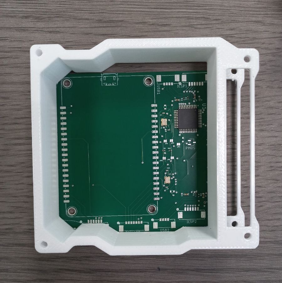
Fig C-10 Second Prototype
C.6.3 Final Product
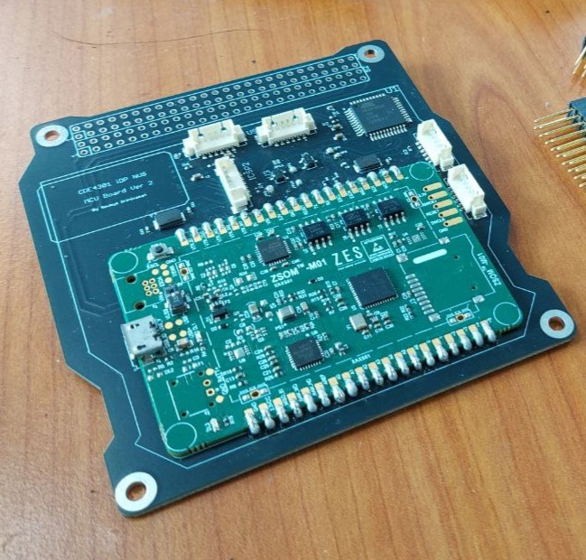
Fig C-11 Final Prototype Inner/Top Side

Fig C-12 Final Prototype Outer/Bottom Side