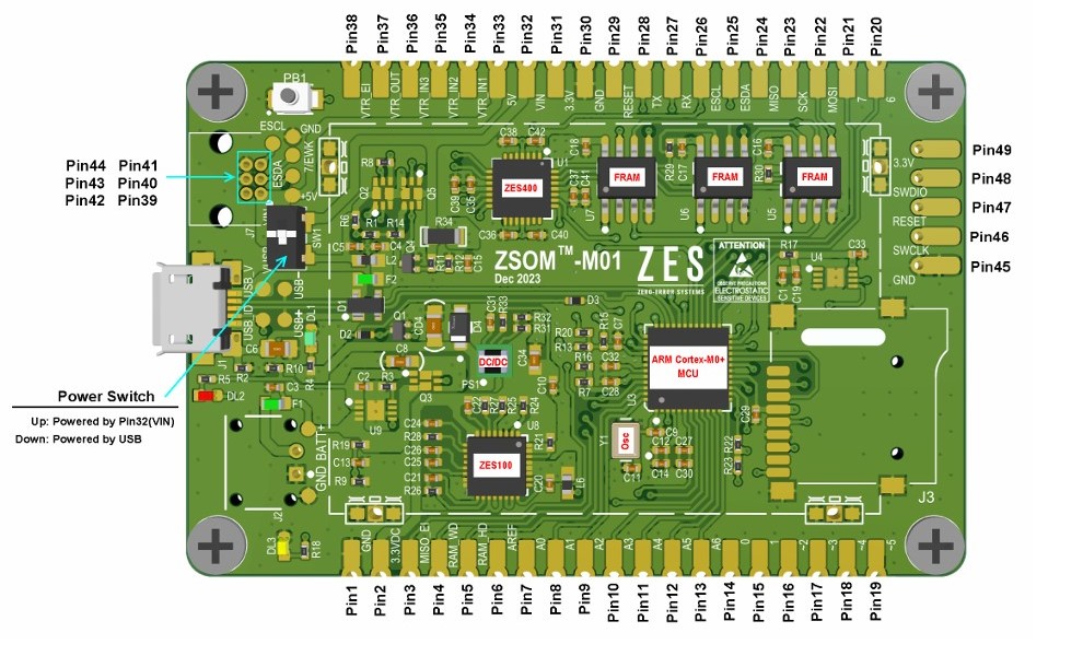
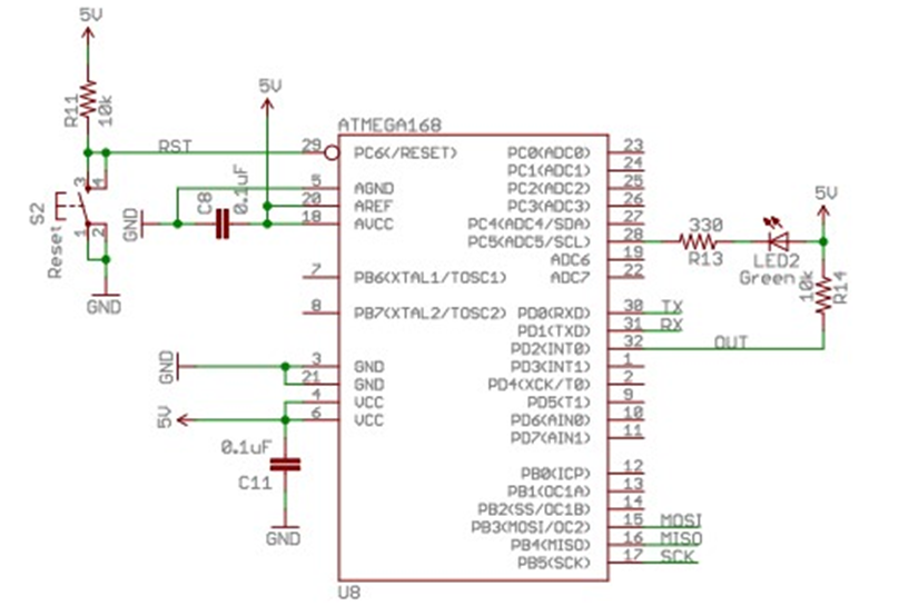
Appendix B1: ZSOM Microcontroller
Design Choice
As specified in the design requirements, a radiation-hardened microcontroller was required to store data reliably. This will ensure that the mission results are reliable.
The ZSOM-M01 was considered because it can be programmed with the Arduino IDE, not only making it easily programmable but also interfaceable with the other chips we wish to experiment with.
Further analysis of the microcontroller’s available storage was conducted to further assure its suitability for the project. This is because as part of a radiation payload, components are to be exposed to high levels of radiation, increasing the risk of SEU occurring. A detailed comparison can be found in Appendix E.
FRAM was deemed suitable to store all the data due to its radiation-hardened status which reduces the risk of data corruption. Additionally, the proprietary EDAC code can correct any bitflips in the FRAM, further enhancing its data protection. The FRAM is also configured in Triple Modular Redundancy with radiation-hardened voters (Zero Error Systems, 2024b). This adds a third layer of protection for its memory contents, making it a suitable choice. The radiation-hardened test summary provided by Zero Error Systems can be found in the appendix.
Since the trustworthy Zero Error Systems meets the requirements of the mission, it has been chosen for the project.
Analysis of Memory Storage Options
| Memory | Pros | Cons |
|---|---|---|
| Flash |
|
|
| SRAM |
|
|
| FRAM |
|
|
Flash storage can help store massive amounts of data. However, flash memory is external to the microcontroller, hence it is not radiation-hardened. It is also known to get corrupted by radiation. This is because radiation removes electrons from the floating gate in flash memory, causing unwanted bitflips (Kay et al., 2017). Hence using flash memory may derail the mission due to the high risk of data corruption. Even if Error and Detection code (EDAC) can help correct data corruption, the code may not be robust enough to handle multiple types of corruption events (Hansen et al., n.d.). Therefore flash memory should be avoided to prevent this potential point of failure.
SRAM is the next viable storage option. However, the data in SRAM gets wiped out if power cycling happens (Awati & Sheldon, 2024). Since there is a high chance that other non-radiation-hardened components experience latchups, the frequency of power cycling may be high. Hence, there would be little to no progress in the mission as the collected data get wiped frequently To avoid this, the SRAM should not be used.
Appendix B2: Radiation Sensor
Design Choice
Several radiation sensors were considered below. These sensors were chosen on their ability to detect the desired charged particles.
| GM Tube | Ion Chamber | Solid State Detector | |
|---|---|---|---|
| Particles | Alpha, Beta, Gamma | Alpha, Beta, but mainly Gamma | Alpha, Beta, Gamma |
| Input Voltage | High | Low | Low |
| Form Factor | Very small and light | Very small and light | Bilkier for more than 1 radiation type |
| Durability | Robust | Fragile when built to detect alpha and beta | vulnerable to radiation damage |
| Ease of Testing | Easy | Easy | Difficult |
A more detailed comparison of the other sensors is in Appendix G.
Geiger-Müller (GM) tubes are preferred in our project to provide radiation data from desired particles that are responsible for SEE. It only requires simple electronics to provide high potential difference across its terminals and to read the signals it produces, making it easy to integrate. They are also considered a cheap relative to other sensors, but they have low energy detection efficiency when receiving high doses of radiation (Matsusada Precision Inc., 2024). However, it is sufficient as the project only needs to quantify the radiation received by the payload, and does not need comprehensive and high-resolution data. The GM tube is also chosen since the other two options are also more vulnerable to damage during space operations, causing a major risk of failure during the mission.
Design Proposition

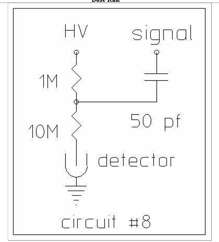
The LND 712 is chosen for our purposes. It requires between 450 to 650V to operate, hence power can be supplied easily with a DC-to-DC converter, making it easy to integrate. The connections required are also very simple, requiring two resistors and a 50pF capacitor. This component, although being one of the largest components in the circuit, only weighs a mere 8g, therefore providing extra allowance on the mass budget for other purposes (LND. Inc., n.d.).
Appendix B3: Proof of Concept
Circuit Layout
Reference was taken from a tutorial on Sparkfun on assembling the circuit components.
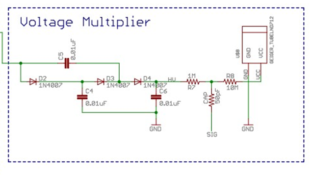
The circuit is then adapted for our project as shown below: 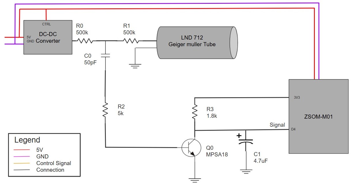
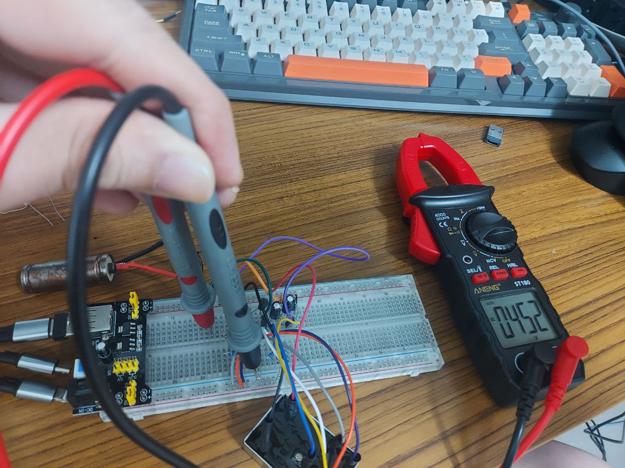
A simple arduino code was then used to enable the Arduino Uno to detect the GM tube signal.
The microcontroller successfully detected the radiation signals from the GM Tube.
This proof of concept validated the following findings:
- Load-independent DC-DC converter provided reliable 500V that is sufficient for GM Tube operations
- Signal conditioning is sufficient, and the signal from the GM is detectable by the microcontroller.
Following form this experiment, further optimizing the circuit components, especially R0, R1, and C0 is required before the custom circuit board can be designed and fabricated
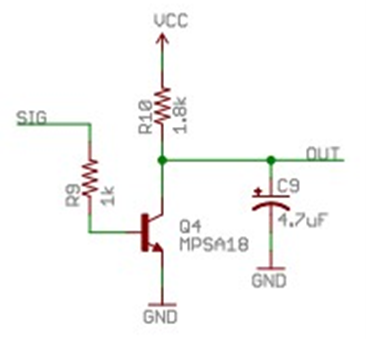
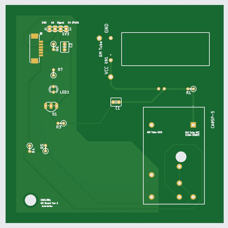
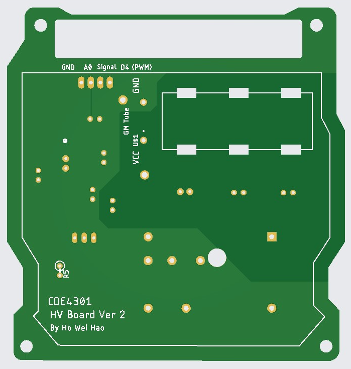
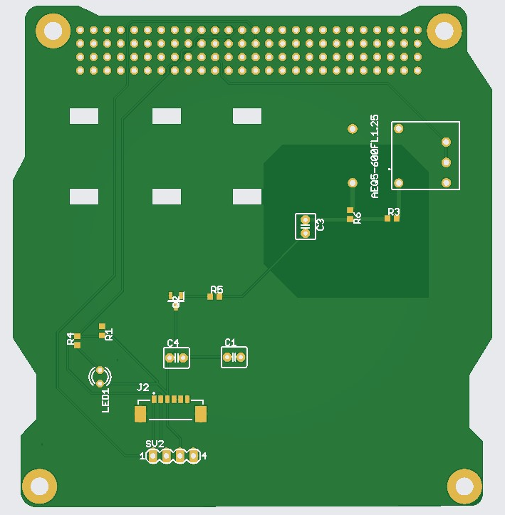
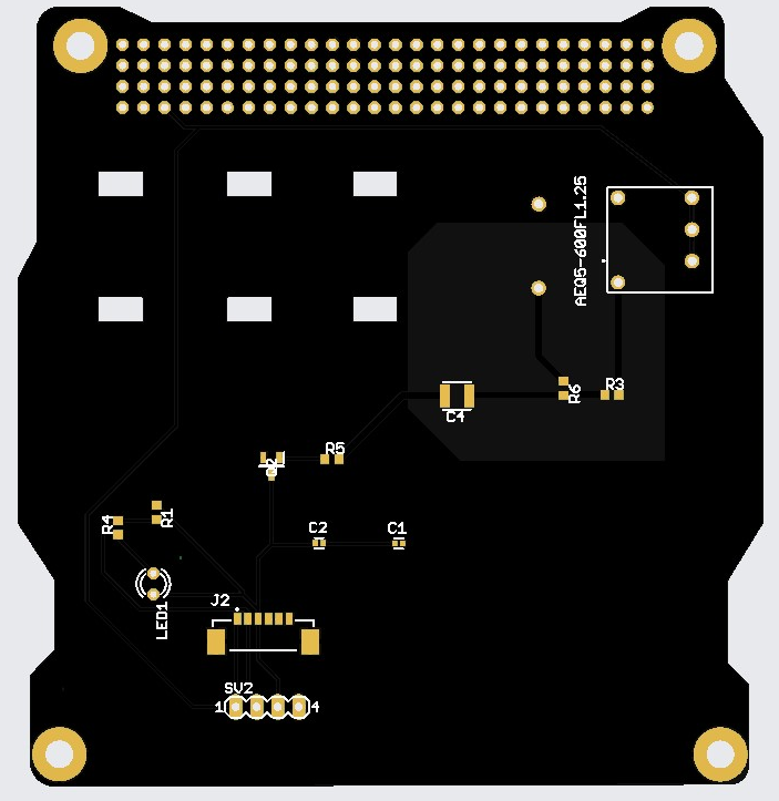
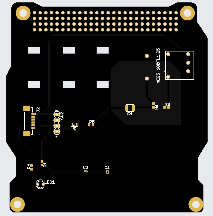
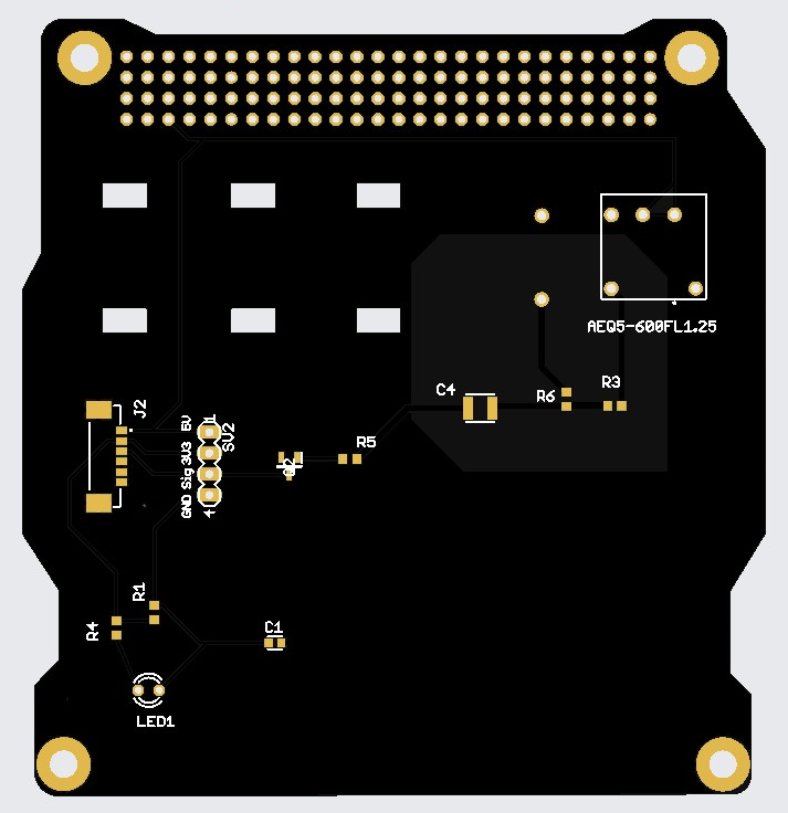
Appendix B4: High Voltage Circuit Design
The high voltage circuit is designed shown: 
The high voltage circuit is made of the following parts:
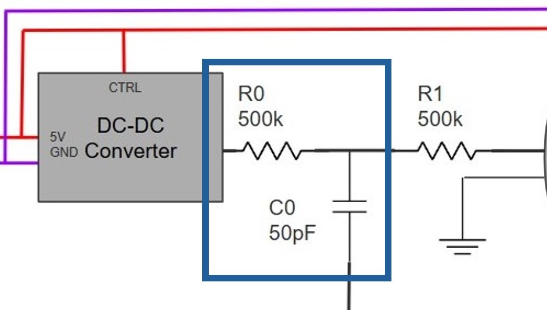
Lowpass Filter (R0 and C0) to prevent signals from interfering with the GM tube.

Highpass Filter (R1 and C0) to filter signals towards the microcontroller, as well as a lowpass filter to prevent Gm tube signals from intefering with the high-voltage source.
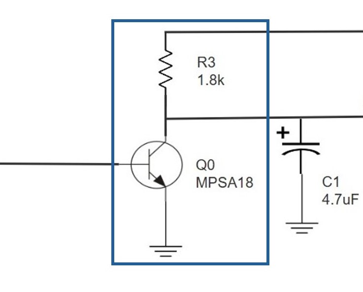
Current amplifier (Q0 and R3) to amplify the current of signals so that the signal becomes detectable by the microcontroller.
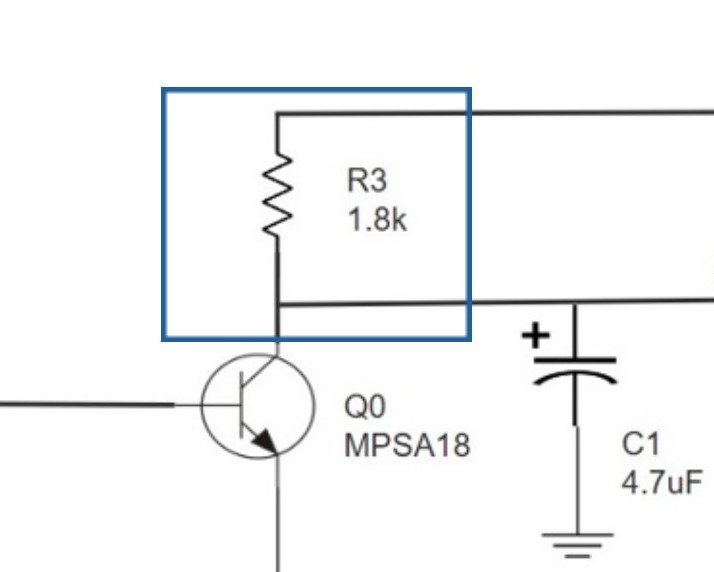
A 3.3V pull-up (R3) to bring the signal line to 3V3 if the line is floating.

Lowpass filter (C1) to clean up signal for reading.
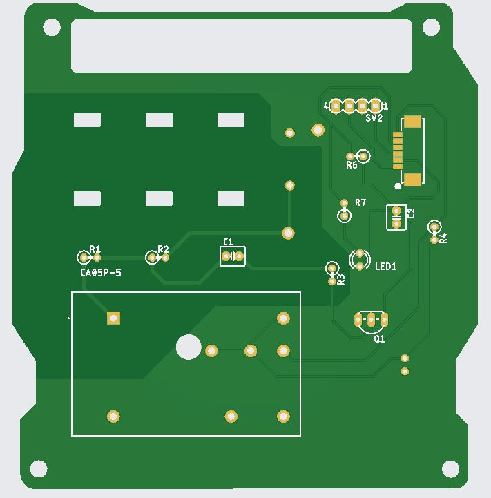
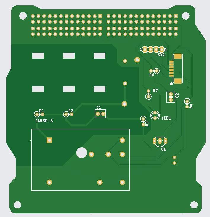
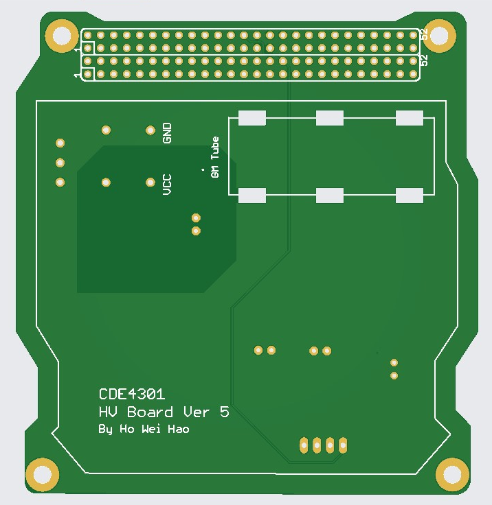
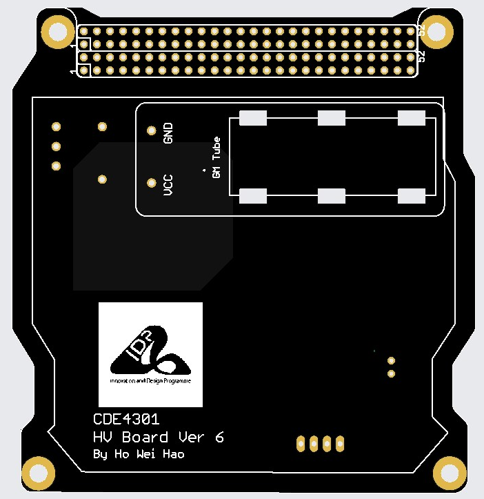
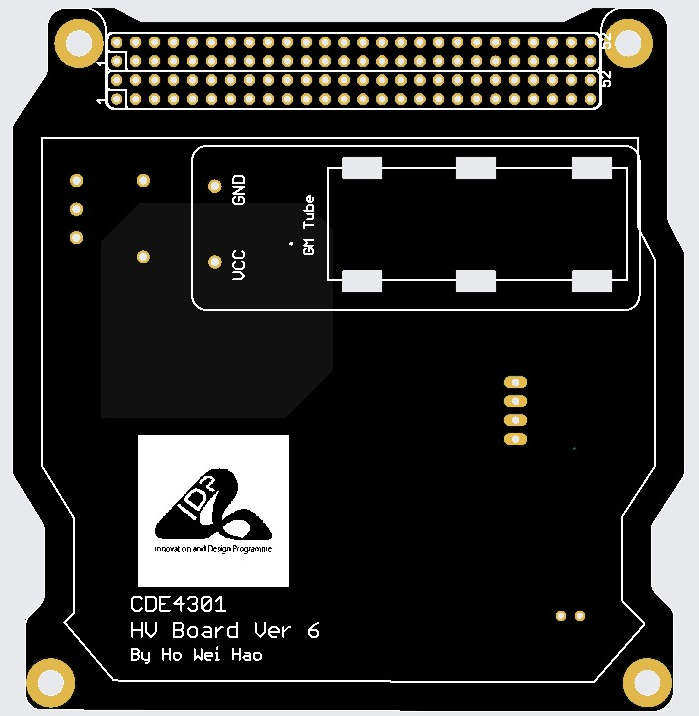
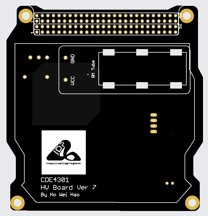
Appendix B5: PCB Design Iterations
The PCB underwent multiple prototype designs to test assumptions and hypotheses, as well as ensure alignment of specifications between the other teammates. The iterations are listed below
Iteration 1
- Place all components on 10cm by 10cm PCB to check for sizing and possible component positioning.
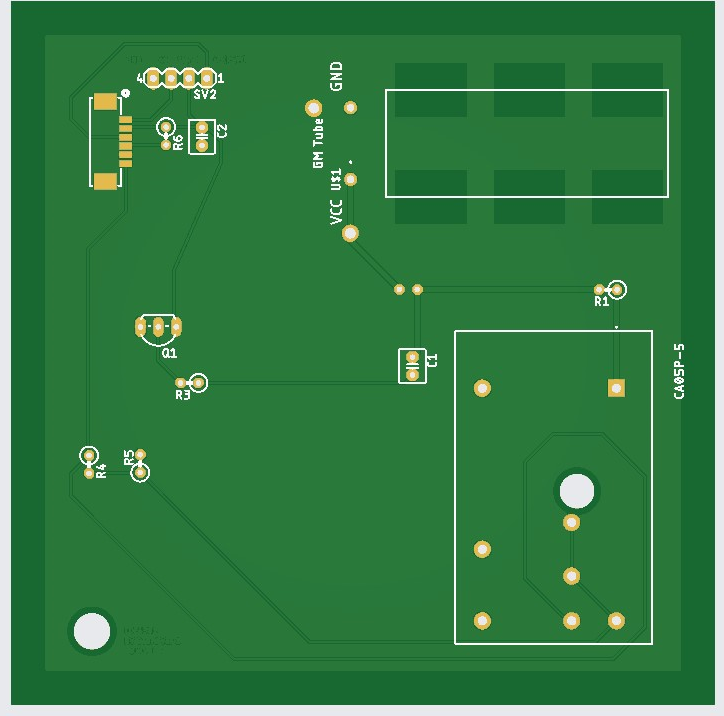
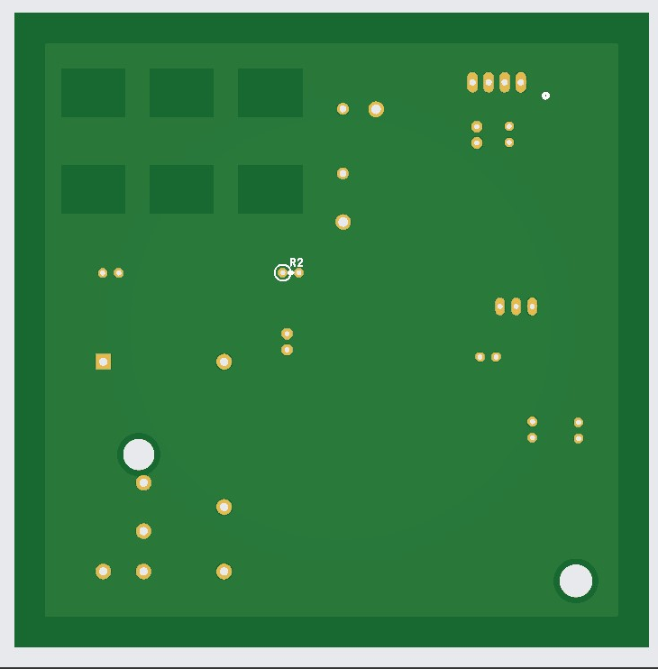
Iteration 2
- Add ground plane clearance around the high voltage lines.
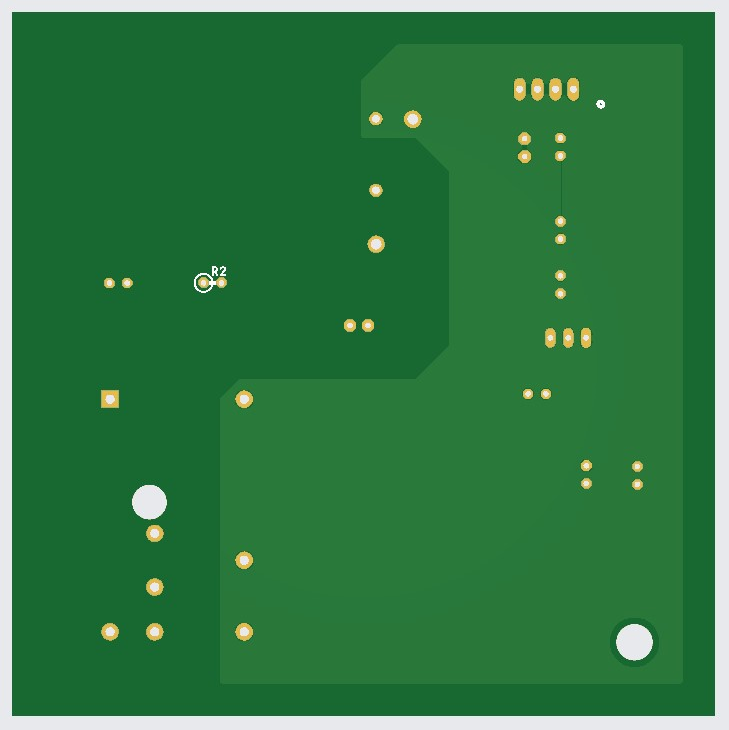
Iteration 3
- Introduced desired shape of the PCB for fit check with shielding and alignment check of the mounting holes.
- Pinstack was modeled as a rectangular hole to ensure that shielding did not obstruct the pinstack location.
- Non-plated through-holes were designed to the sides of the GM tube footprint for cable-ties to loop through and bound the GM tube to the PCB.
Iteration 4
- Add pinstack footprint and sizing for fit check with mechanical.
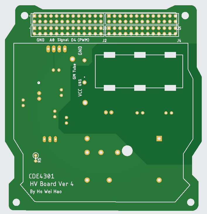
Iteration 5
- Converter was updated to a space suitable one and shifted to be closer to the GM tube to shorten the high voltage lines.
- Pinstack footprint was changed to reflect the actual 52 position pinstack we will be using, rather than two 26 position pinstacks per row.
- Conducted pinstack alignment check with low voltage PCB.
Iteration 6
- PCB colour changed to black to reflect the final colour choice.
- Finalised relative positioning of components.
Iteration 7
- Edited converter footprint.
- Edited capacitor value on lowpass filter on signal net
Iteration 8
- Final check on all components placement and traces.
- Shifted the converter closer to the shielding for better thermal contact between converter thermal interface material, and shielding
Appendix B6: Microcontroller Code
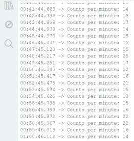
The code attaches an interrupt service provider to pin D4 and configures it to be in input pull mode. The D4 pin will be triggered by the falling edge of the signal from the GM tube. When the pin is triggered, the microcontroller counts the pulse. After 1 minute, the microcontroller resets the count to 0 for the next minute. A debouncer is added to ensure that the microcontroller does not count unstable signals multiple times.
The code is as follows:
volatile int count = 0;
volatile unsigned long lastInterruptTime = 0;
uint32_t start;


void setup() {
  pinMode(4, INPUT_PULLUP);
  Serial.begin(9600);


  Serial.println("Start");


  // Attach interrupt on pin 2 (Interrupt 0) for falling edge detection
  attachInterrupt(digitalPinToInterrupt(4), handleInterrupt, FALLING);
  start = micros();
}


void loop() {
  // Check if 1 second has passed
  if (micros() - start >= 60000000) {  // 1,000,000 µs = 1 second
    Serial.print("Counts per min: ");
    Serial.println(count);


    // Reset count for the next second
    count = 0;
    // Reset start time
    start = micros();
    interrupts();
  }
}


// Interrupt Service Routine (ISR)
void handleInterrupt() {
  unsigned long interruptTime = micros();


  // Debounce: Only count if >200 microseconds have passed since last pulse
  if (interruptTime - lastInterruptTime > 10000) {
    //Serial.println("Detected!");
    count++;
    lastInterruptTime = interruptTime;
  }
}