
Sowmya Srinivasan
Year 4 Electrical Engineering
A0246190H
3. The Bit Flip Experiment
3.1 Objectives, Scope of Work & Deliverables
Objective: The complete implementation of the Radiation-SEU Correlation experiment.
The Deliverables: Proposal of Radiation-SEU Correlation Experiment PCB Implementation of the Proposed Experiment for the Payload.
3.2 Background & Research Gap Identification
3.2.1 The Reason For Monitoring Bit Flips
Bits that represent either data or programs, are stored in computer memory as charge. Different memory devices deal with different levels of charge to store bits. When ionizing particle radiation strikes a material, it can alter this charge, changing 0’s to 1’s and vice versa. These flips cause corruption in both program and data memory and are called SEU (Baraniuk, 2022).
3.2.2 Bit Flip Experiments Carried Out
While some microcontrollers have been in LEO, the only experiment carried out and available online is by Utah State University (Olsen et al., n.d.), but the experiment was conducted in a lab environment, and the data collected was limited. The diagram below summarizes the current state of research on bit flips in space.
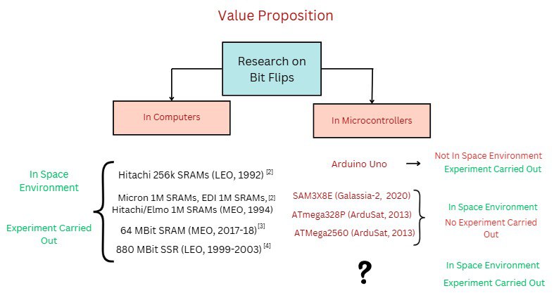
Hence, there is a gap in research about bit flips in microcontrollers in space environment.
While data from computers can give cubesat developers a rough idea of what to expect, the data cannot be confidently used for microcontrollers. Hence, our payload intends to bridge this gap in research and benefit our stakeholders.
3.3 Design Process
3.3.1 Concept of Experiment
Basic Idea
- The experiment comprises microcontrollers of the same kind being sent to space, both shielded and unshielded.
- While having multiple microcontrollers with different shielding materials or thickness would be ideal, the space constraint and data budget limit permit only 2 microcontrollers to be used.
- Hence, one microcontroller is unshielded, while the other is shielded (shielding is from Mingchuan).
- Both the microcontrollers under experiment would experience bit flips, and every minute, a central microcontroller (selected by WeiHao) gathers the data on bit flips from them. The reasoning for a 1 minute interval is in Appendix Section D.1
- The central microcontroller then computes the error count by comparing the fixed pattern with the received pattern and also stores either error indices or a 10% sample of the SRAM to memory. (information to be stored is decided by Richard)
- The radiation counts per minute is measured by a Geiger Muller tube (selected by Wei Hao)
Possible Inferences From Experiment Data
- The error count of the unshielded microcontroller would tell us the extent of radiation tolerance of the chosen MCU.
- Comparing the error count of the unshielded microcontroller with the Radiation CPM of the Geiger Tube would allow us to quantify the correlation between SEU and particle radiation in LEO.
- Comparing error counts of the shielded and unshielded microcontrollers would quantify the effectiveness of the shielding method.
3.3.2 Design Specifications
| Feature | Specification | Reasoning |
|---|---|---|
| Current Consumption | <100mA | The central microcontroller (ZSOM) is rated for 500mA, including its own operation. It is reasonable that we should draw <20% of the total current resource. |
| Operating Voltage | 3.3V | The ZSOM supplies power at 3.3V, and has logic voltage of 3.3V as well. |
| Duration of Data Transfer | <12s | The experiment is to be conducted every minute. Since other tasks need to be done in that time, only <20% of the time should go for data transfers. |
| Size of Experiment Payload | <1088 mm2 in Area <5 mm in Height | Derived from payload layout. A very rough sizing check is in Section 3.4, Appendix. |
| Minimum Size of Memory to count bit flips | >1 Kb | Up to 10 upsets can happen over 1kB per day (Matthews, 2021). <1 kB means too little information from the experiment. |
| Maximum Size of Memory to count bit flips | <=2.56 Kb | Restricted by the data budget of only 256 bytes per microcontroller. A minimum sampling of at least 10% is desired for good data collection. |
3.3.3 Design Choices Reasoning
For each aspect of the experiment, a design choice had to be made, as elaborated below.
The Memory Device
The Ideal Case: Easy to read, Highly susceptible to bit flips, Size of 1 to 2.56 kB, Easy to reset, does not lose data upon power cycle due to SEL .
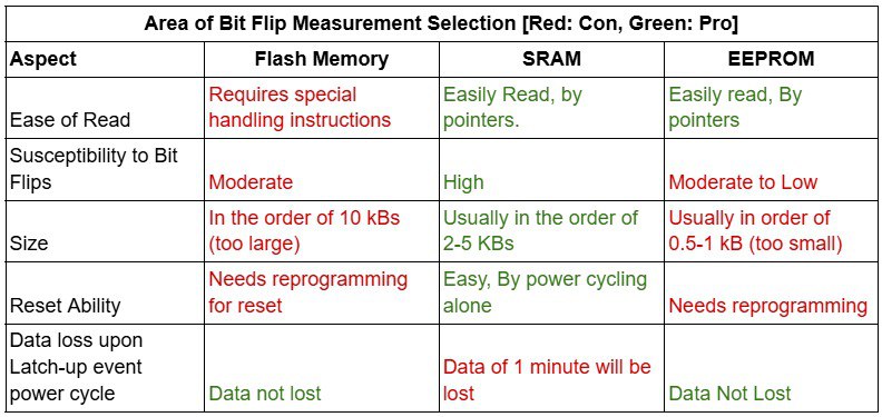
Due to the highest number of positives, the SRAM was chosen as the memory device. The one drawback, that is of data loss upon occasional latch-up events, is deemed to be worth the benefit of a simpler reset, which will be needed more often than the latch-up events.
ZSOM to Microcontroller Communication
The below table lists the communication peripherals on the ZSOM board and its availability or relevance for this experiment.
| Communication Interface | Can it be used for this experiment? |
|---|---|
| SPI | No. SPI of the ZSOM is being used to implement CAN protocol and interface with the OBC, which shouldn’t be interfered with. |
| UART | No. UART is a peer-to-peer protocol. The experiment needs a bus protocol for 2 ATMegas to communicate to the ZSOM. |
| I2C | Yes. It is not being used for any other purpose and is a bus protocol. Also, data transfer speed is sufficient. |
Due to I2C being the only interface on the ZSOM that is available for use and supports multiple devices, I2C is chosen as the communication interface between the ZSOM and the ATMegas.
Since it is known that I2C can face problems in the space environment, the experiment incorporates a timeout feature followed by bus reset and/or power cycling to provide robustness to the transfer of data.
Further elaboration on the various issues faced by I2C and our approach towards managing it elaborated on in the Appendix, Section D.2
The Microprocessor
The Ideal Case: Has I2C Interface, a readable SRAM, NO flight heritage, SRAM in 1-2.56 kB size range, high probability of use in future missions
After applying an initial filter of SRAM sizes, availability of documentation, popularity, and presence of unique features, the following 3 microprocessors were shortlisted for a good demonstration of the reasons for selection.
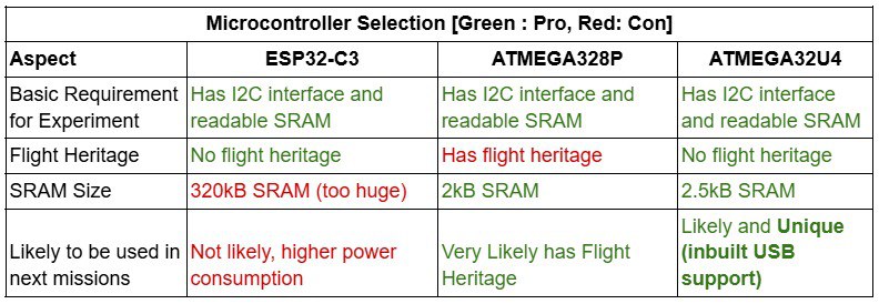
Hence, ATMega32U4, having the most positives, is selected as the Microcontroller under experiment.
The appendix further elaborates on The reasoning towards not selecting other microcontrollers with USB support (Appendix Section D.3) Explanation of the flight heritage relevance of the ATMega328P (Appendix Section D.4)
Other Components
| Component | Choice | Reasons |
|---|---|---|
| Power Source for ATMegas | 3.3V from ZSOM, with SEL protection | The ZSOM provides protection against latch up events so that the microcontrollers do not suffer permanent damage. ZSOM has a power cycle implementation after latch-up detection. |
| Power Cycling Method | PMOS as a digital switch | Simple and known implementation. Provides digital control. Can meet the current and voltage specifications. |
| Bootloader | Caterina by Sparkfun | Supports 3.3V and 8MHz Clock. Supports programming by D+ D- pins. In use by Sparkfun ProMicro. |
| Bootloader Upload | ICSP & Arduino as ISP | Very common, reliable method. |
| Program Upload | D+ D- USB | Only 2 additional pins to the ICSP header in the PCB. In use by SparkFun Pro Micro. |
3.3.4 Design Choices Summary
The table below summarizes the final choices made for each component.
| Requirement | Component Choice |
|---|---|
| Microprocessor Chip For Experiment | ATMega32U4 |
| Area to Observe Bit Flips | SRAM |
| ATMega to ZSOM Communication | I2C Protocol |
| Robustness Method | Bus Reset and Power Cycling |
| Bus Reset Implementation | 9 Pulses on SCL after Timeout (the usual I2C method for reset) |
| Power Cycling Implementation | PMOS Switch |
| Power Source of ATMegas | ZSOM SEL protected, 3.3V pin |
| Bootloader | Caterina by SparkFun |
| Bootloader Upload Method | ICSP |
| Program Upload Method | D+ D- Inbuilt USB |
| Reference Microcontroller Board | SparkFun Pro Micro 3.3V, 8MHz |
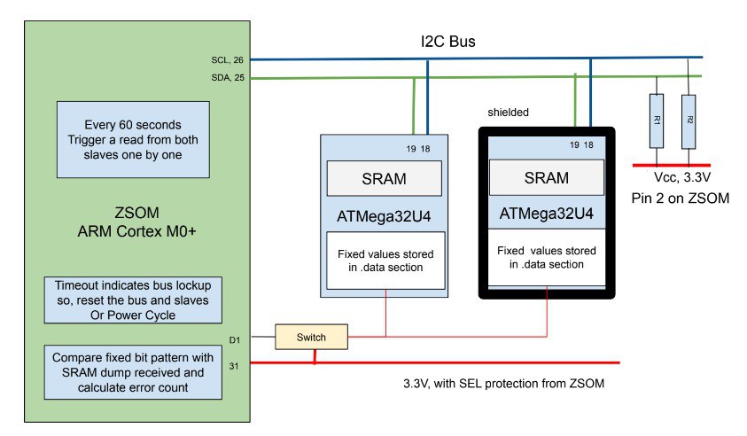
3.3.5 Final Design of Experiment
The diagram below illustrates the working of the experiment, using the final design choices. As bit flips occur in the ATMega32U4’s, their SRAM Dump will reflect them.
3.4 Prototyping and Testing
3.4.1 Prototyping Objectives
- To provide proof of concepts used in the experiment.
- To collect rough estimates of power consumption and data transfer duration.
- To verify repeatability of the experiment.
3.4.2 Description of Prototype
The below table describes how each aspect was implemented in the prototype.
| Feature | Implementation in Prototype |
|---|---|
| Central Microcontroller | SparkFun Pro Micro 3.3V, 8MHz |
| MCUs under test | 2 x SparkFun Pro Micro 3.3V, 8MHz |
| PMOS Switch | SMD PMOS soldered onto veroboard + wires |
| I2C Bus | On the breadboard + wires |
Pictures and Specifics of the prototype and some verifications/characterizations are present in Appendix Section D.5
3.4.3 Verifications of Proof of Concepts
| Verification Attempt | Outcome |
|---|---|
| ICSP Bootloader Flashing | Bootloader Flashed successfully |
| Code Flash Through D+/D- | Code Flashed Successfully |
| Storing fixed Data in SRAM | Consistency in the fixed bit pattern observed within the applicable range of memory addresses |
| Trigger Based Data Transfer Over I2C | Data Transfer completed successfully |
| Power Cycling Implementation | Implemented Successfully |
| Bus Lockup and Reset Implementation | Implemented Successfully, Master can detect timeout and reset |
| Repeatability | The implementation shows the same behavior over multiple runs |
3.4.4. Data Gathered Through Testing
| Characteristics | Value, Unit | Within Specification? |
|---|---|---|
| Current Consumption of 1 Pro Micro | 11 mA | Yes (Reasonable) |
| Achieved Supply Voltage for ATMega32U4s | 3.29 V (min) | Yes (Nearly 3.3V) |
| Current Consumption of the Entire Prototype Circuit [Lead Pro Micro + 2 Pro Micro under Test] | 33 mA | Yes (<100mA) |
| Time to Receive, Count Errors and Create 10% array for 1 SRAM Dump | ~1 s | See row 6 |
| Time to Complete Full Operation [Receive, Count Error, Create 10% Array, Both ATMegas] | ~2.3 s | See row 6 |
| Time for 1 Bus Reset + 1 Power Cycle | ~8 s | See row 6 |
| Worst Case Time [1 Bus Reset + 1 Power Cycle + 1 Full Operation] | ~10.3 s | Yes <12s |
The expected differences in functionality of the prototype and the final PCB implementation are as follows
- ZSOM current consumption will be different from the SparkFun Pro Micro that is currently being used as the Master.
- The Power consumption of the ATMega32U4 will also differ in PCB due to possible differences in the component models being used.
- The breadboard capacitances contribute to the bus capacitance and hence currently, data transfer speed of I2C is lower than would be on a PCB.
Despite these differences the testing has provided rough estimates that verifies the feasibility of the experiment.
3.5 Moving Forward
The work achieved thus far is the first deliverable, “Proposal of Radiation-SEU Correlation Experiment”. Additionally, the functionality of concepts and ability to adhere to specifications is verified.
Moving forward, following are the key milestones or tasks pending.
Milestone 1: Design of PCB Schematic and Layout of the prototype Intermediates:
- First iteration of the PCB, followed by Testing & Improvements
- Second iteration of the PCB, Testing and Characterization
Milestone 2: Integration with the other Electronics Member Intermediate : Testing and Improvements of the Combined PCB
Milestone 3: Integration with Mechanical and Software sections Intermediate: Combined Testing and Improvements or optimization (if needed)
Final Milestone: Final Checks before deeming the payload flight ready.
For the temporal work plan, kindly refer to the combined table in the “Future Work” section of this report.