
Richard Loong Cheng Jun
Year 4 Computer Engineering
A0233496X
4. Software Development
4.1 Scope of Work
As the main software developer of the team, my scope of work can broadly be described as the following:
- Create data structures to optimise the use of the onboard data storage
- Select electrical connectors to interface with the parent satellite
- Implement the necessary protocols to enable communication with the parent satellite
- Integrate software from the rest of the team into a single software package
4.2 Design Objectives
The main objectives of my part of the project include:
- Reading data from the payload’s onboard storage
- Receiving data from the parent satellite
- Sending data to the parent satellite
- Handling commands received from the parent satellite
4.3 Design Requirements
The primary design requirement for my part is to ensure that our payload can be integrated with the parent satellite. Therefore, the specifications I have to meet are entirely dependent on our rideshare partner.
At the time of writing this report, our team does not have a confirmed rideshare partner yet. As such, I do not have a finalised list of specifications that I can use to base my design choices on. However, we do have a technical partnership with In-Space Missions, which is a subsidiary of BAE Systems, and their Faraday Dragon program.
Through this partnership, I have access to some of the specifications and documents for the Faraday Dragon spacecraft such as their Payload Integration Emulator (PIE) user guide and their Interface Control Document (ICD). Additionally, there are active communication channels between us and the Faraday Dragon team.
Therefore, I am basing many of my design choices on the Faraday Dragon spacecraft’s integration requirements. However, some details such as mission parameters are still not determinable as there is not a specific mission to base our experiments on.
4.4 Design Choices
4.4.1 Data Frame
Experiment data will be stored in the 32kB FRAM of the primary MCU. The actual experiment duration will depend on our parent satellite, but for development purposes, I am assuming the following mission parameters:
- 60 min total experiment duration
- 01 min interval between readings
Each experiment reading will be stored as a single data frame. Under these parameters, each data frame can use a maximum of 533 bytes of storage. The planned data frame uses up to 524 bytes of storage.
| Epoch Time | Particle Count | Error Count #1 | Error Count #2 | Experiment Data #1 | Experiment Data #2 |
|---|---|---|---|---|---|
| 4 bytes | 4 bytes | 2 bytes | 2 bytes | 256 bytes* | 256 bytes* |
| signed int | unsigned int | unsigned int | unsigned int | custom data type | custom data type |
Epoch Time
The time the reading was taken. This timestamp is retrieved from the parent satellite as our payload has no onboard clock.
We are using Unix epoch time conventions, based on the epoch of 1 Jan 1970, 0000hrs UTC/GMT. Unix epoch is widely implemented in software libraries, making it the most convenient epoch time to use. The Year 2038 problem that comes with the Unix epoch is unlikely to be an issue as we expect our mission to have ended by then.
The epoch time is stored as a 32-bit (4-byte) signed integer.
Particle Count
The number of particles counted by the Geiger–Müller (GM) tube. This is measured in counts-per-minute (CPM).
The particle count is stored as a 32-bit (4-byte) unsigned integer.
Error Counts
The number of bit flips detected in each MCU’s SRAM.
The ATmega32U4 MCU has 2.5kB of SRAM, which is 20480 bits, which fits comfortably in a 16-bit data type so even in the event that every single bit flips, all errors can be counted.
The error count is stored as a 16-bit (2-byte) unsigned integer for each MCU.
Experimental Data
This is the data that scientists can use for research beyond the scope of our project.
The final data allocation for this research is subject to change. Based on a 60-min experiment duration with 1-min intervals between readings, 256 bytes can be allocated to each MCU.
The contents of the experimental data is not yet finalised, but it is designed to allow for the recreation of the SRAM back on earth, complete with errors. This is achieved by storing the location in memory of each flipped bit.
The ATmega32U4 uses 12-bit memory addresses, with each address representing 1 byte. We append an additional 4-bits to the address to represent the specific bit that has flipped. This means each bit can be represented by a 16-bit (2-byte) address.
With 256 bytes allocated to each MCU, up to 128 flipped bits can be recorded and stored. Assuming 10 bit-flips per day per 1 kB of SRAM, we expect a mean of 25 bit-flips per day per MCU, or 1 bit-flip per 1 hour experiment. The 128 error capacity should be sufficient to record all errors that occur.
Another benefit of this method is that less than 256 bytes will be used if there are fewer bit-flips, allowing the experiment to extend beyond the current 1-hour duration if necessary without any memory limitations.
4.4.2 Electrical Interfaces
The electrical interfaces are the electrical connections between the payload and the parent satellite. These include power delivery and communications. There are a total of 6 pins needed for this interface:
- Low Voltage (LV) power delivery: 5V and GND
- High Voltage (HV) power delivery: 5V and GND
- Communications: CAN H and CAN L
The LV and HV components are on separate PCBs for isolation, and are preferably on separate power delivery circuits for the same reason.
2 different physical interfaces are being developed that can be toggled between before launch in order to accommodate possible rideshare requirements. A jumper will be used to select between the two interfaces. The unused interface will be electrically disconnected from the rest of the payload.
PC104 Pinstack
This is the 104-pin header that can be commonly found on cubesat components. There is no standard pinout for this header so the “manufacturer default” pinout from Gomspace products is being used:
| Connection | Pin |
|---|---|
| LV 5V | H2 Pin 25 |
| LV GND | H2 Pin 31 |
| HV 5V | H2 Pin 26 |
| HV GND | H2 Pin 32 |
| CAN H | H1 Pin 1 |
| CAN L | H1 Pin 3 |
This pinout is subject to change depending on rideshare specifications.

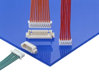
Molex Picoblade
For rideshares without the PC104 pinstack, the picoblade connector will be used. The picoblade connector supports up to 2.0A per connection and has flown on previous spacecraft.
4.4.3 Communication Protocol (Layer 2)
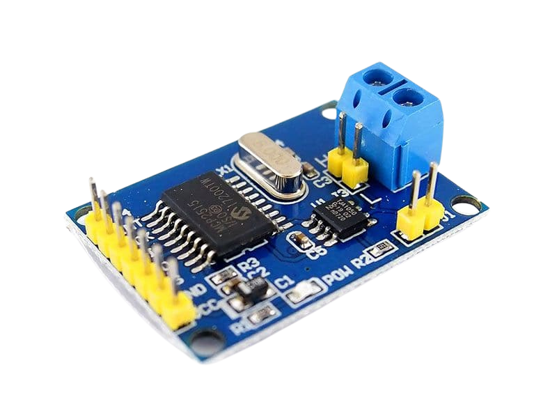
CAN is being used as the layer 2 communications protocol. It is widely used and is one of the protocols used by the Faraday Dragon rideshare. The primary MCU (ZSOM) does not have any onboard CAN hardware, so an external module is needed.
The CAN Controller is the MCP2515 and the CAN Transceiver is the TJA1050 and there are many software libraries available that support these two chips. The CAN Controller connects to the SPI of the primary MCU.
4.4.4 Communication Protocol (Layers 3+)
Cubesat Space Protocol (CSP) is used as the higher layer communications protocol. It is a protocol stack following the TCP/IP model, and is used as part of the messaging system on the Faraday Dragon rideshare.
On top of CSP, the Faraday Dragon uses an Abstract Messaging Service (AMS) that is used to send Service Operations Messages that correspond to the various services of the spacecraft such as timestamp sharing.
4.4.5 Payload Interface Emulator (PIE)
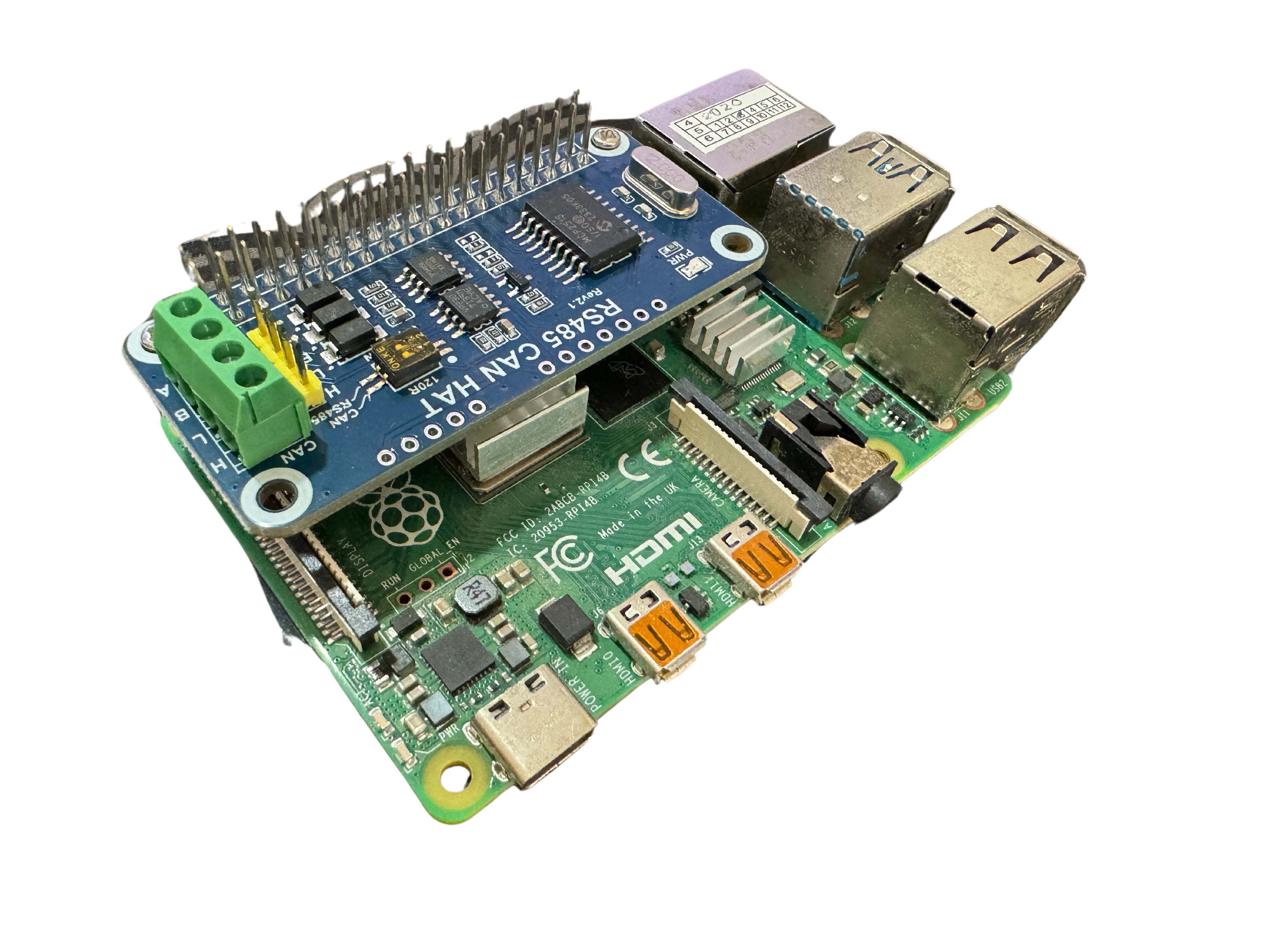
For testing, a Raspberry Pi 4B with the Waveshare RS485 CAN Hat is being used to emulate the Onboard Computer (OBC). CAN is set up as a network interface and packets can be sent via command line. Controlling the PIE is done over the network via SSH.
The operating system running on the PIE is Raspberry Pi OS (32-bit)
4.5 Implementation and Testing
4.5.1 Data Frame Reading Test
Sample data was successfully written and read from the FRAM.
4.5.2 PIE Setup
The PIE was set up as per the instructions in the PIE User Guide provided by the Faraday Dragon team and the Waveshare RS485 CAN Hat User Guide.
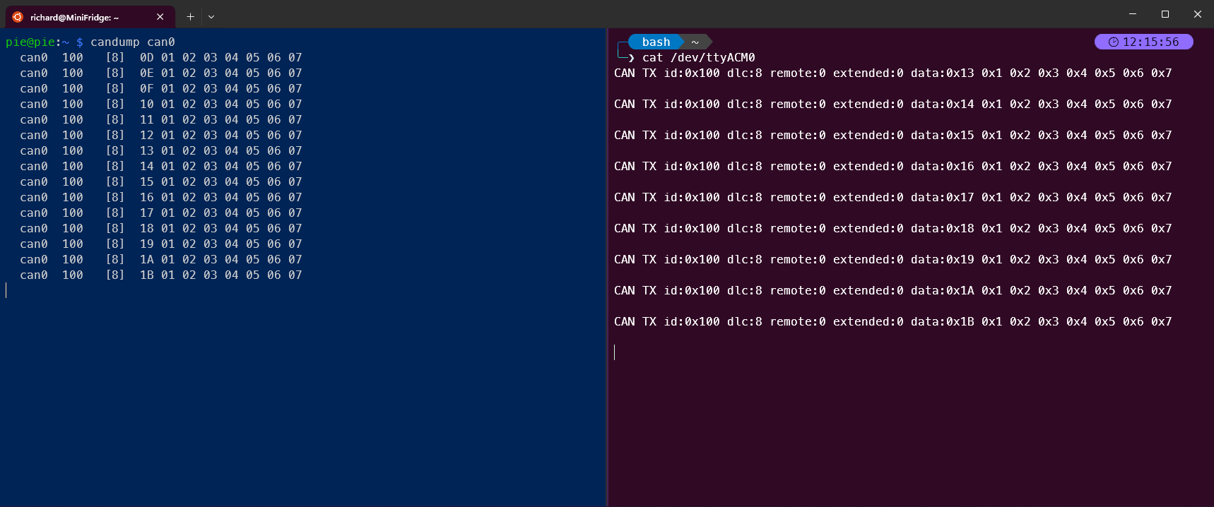
The CAN interface was tested and proven to be functional, able to both send and receive CAN frames via command line on the loopback interface.
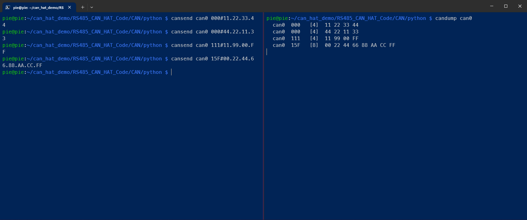
4.5.3 Serial Data transfer via CAN
CAN frames were successfully sent and received between the PIE and the primary MCU. The AA_MCP2515 library was used on the primary MCU as this library allows for easier customisation of pinouts and changing frame IDs.
4.5.4 CSP Installation on PIE
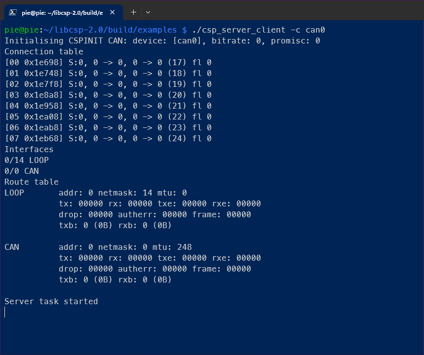
CSP was successfully installed on the PIE, following the instructions in the documentation via the meson build system. Examples were successfully built and the server-client example was able to run on the loopback interface.
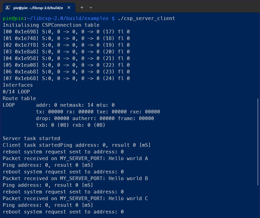
The same server-client example could be started on the CAN interface, but no example messages are sent when only 1 client is on the network, so full functionality could not be verified.
4.5.5 CSP Installation on MCU
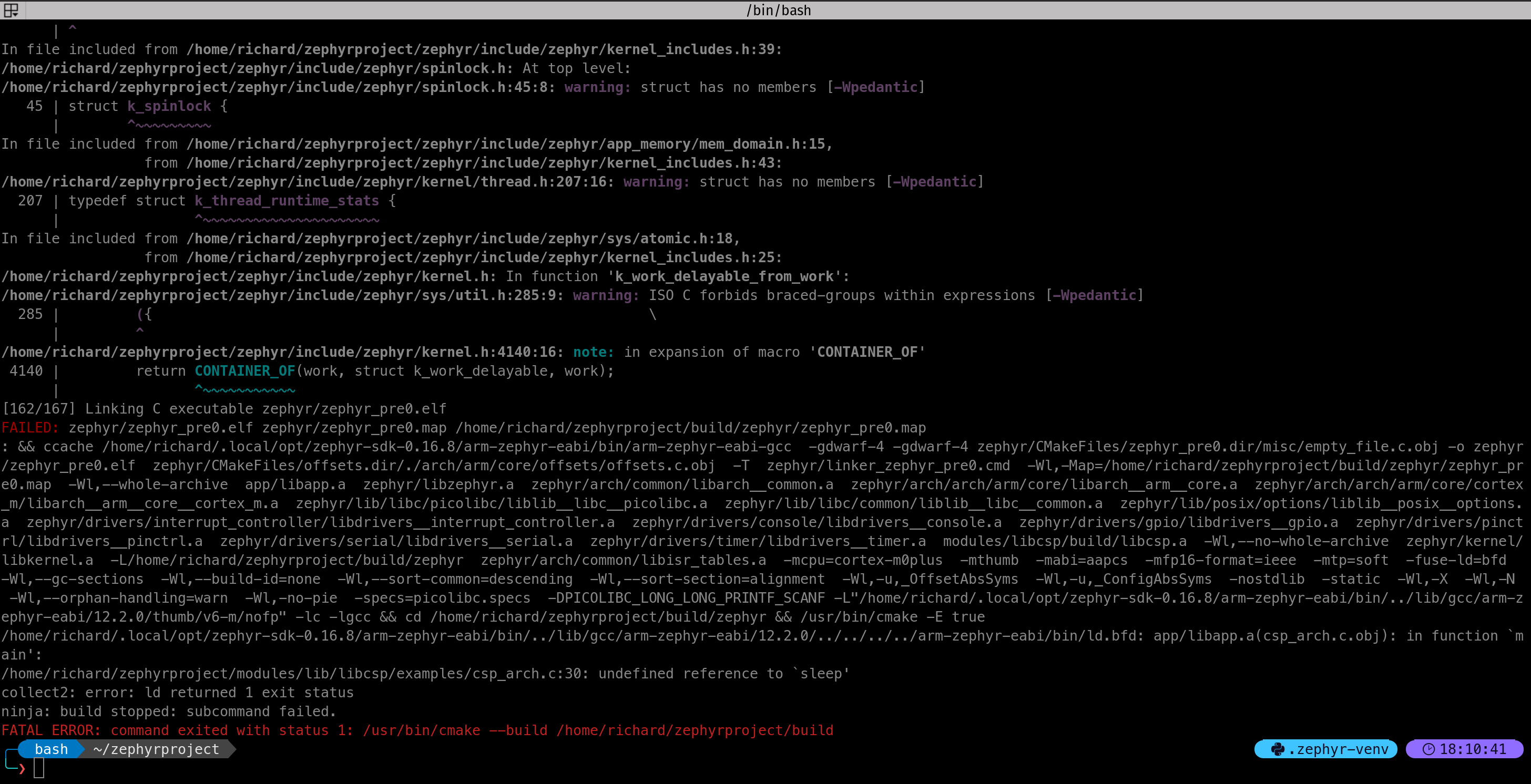
CSP could not be installed on the primary MCU.
Based on the official documentation, CSP has been ported to FreeRTOS, Zephyr and Linux. CSP was able to run on Linux as shown in the PIE, but Linux is not suitable for use on an MCU. Both FreeRTOS and Zephyr are supported by the Cortex-M0+ on the primary MCU and both have successfully run example code without CSP.
There are no instructions available for using CSP on FreeRTOS, and attempts and doing it without instruction have failed as the default build appears to rely on certain Linux system functions that do not exist on FreeRTOS.
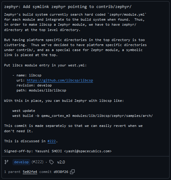
There is a commit in the CSP GitHub repo that provides instructions on building a CSP example for Zephyr, but the build process failed.
4.6 Future Work
- Hex/Bin interpreter program to convert data to human-readable format
- All expected functionality available via conventional CAN
- Integrating other experiment code for ZSOM MCU
- Testing the Integrated Code
- Finalise decision on which RTOS to use with CSP
- Modifying protocol stack to fit rideshare specifications